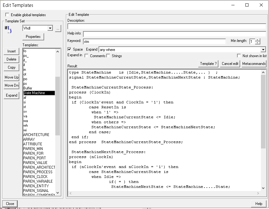
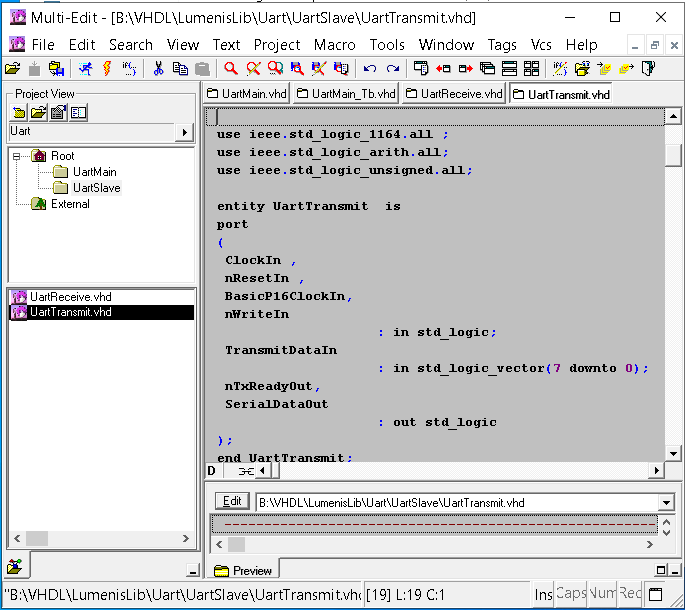
For my VHDL designs   I use Multi Edit ver.9.1 editor with very friendly
user interface and much capability editing tools.

  This editor have many build in VHDL template with option to edit it or
add custom templates.

 For using template user need type keyword and space. Attached Vhdl.tpt
file with my custom templates.

 User can also build project for easy looking for files of project for
editing.
Attached files:
-

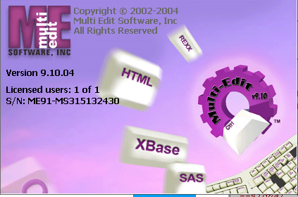
MultiEditTitle.PNG
67 KB -

VHDL_Template.PNG
11 KB -

MeProject.PNG
25 KB
New VHDL file template :

Keyword : new_file<SPACE>
1 | --------------------------------------------------------------------------------
|
2 | --
|
3 | -- Title :
|
4 | -- Design :
|
5 | -- Author :
|
6 | -- Company :
|
7 | --------------------------------------------------------------------------------
|
8 | -- File : xxxxxx.vhd
|
9 | -- Generated : Jun 20 2020
|
10 | --------------------------------------------------------------------------------
|
11 | -- Description :
|
12 | --------------------------------------------------------------------------------
|
13 | -- Revision History :
|
14 | -- -----------------------------------------------------------------------------
|
15 | -- Ver :| Author :| Mod. Date :| Changes Made:
|
16 | -- v1.0 | :| 20/06/20 :| Automatically Generated
|
17 | -- -----------------------------------------------------------------------------
|
18 | library ieee ; |
19 | |
20 | use ieee.std_logic_1164.all ; |
21 | use ieee.std_logic_arith.all; |
22 | use ieee.std_logic_unsigned.all; |
23 | |
24 | entity NameEntity is |
25 | port
|
26 | (
|
27 | ClockIn , -- General Clock |
28 | nClockIn , -- General not Clock |
29 | ResetIn , -- General Reset active High |
30 | `PortName`, -- Port description |
31 | `PortName`, -- Port description |
32 | `PortName` -- Port description |
33 | : in std_logic; |
34 | |
35 | `PortName` -- Port description |
36 | : in std_logic_vector(`MaxValue` downto `MinValue`); |
37 | `PortName`, -- Port description |
38 | `PortName`, -- Port description |
39 | `PortName` -- Port description |
40 | : out std_logic; |
41 | `PortName`, -- Port description |
42 | `PortName`, -- Port description |
43 | `PortName` -- Port description |
44 | : out std_logic_vector(`MaxValue` downto `MinValue`) |
45 | );
|
46 | end NameEntity; |
47 | |
48 | architecture ArchNameEntity of NameEntity is |
49 | |
50 | signal `SignalName` : std_logic; |
51 | signal `SignalName` : std_logic_vector(`MaxValue` downto `MinValue`); |
52 | signal `SignalName` : integer range `MinValue` to `MaxValue`; |
53 | |
54 | begin
|
55 | |
56 | end ArchNameEntity; |
New process template :

Keyword : pps<SPACE>
1 | Name_Process: |
2 | process (ClockIn ) |
3 | begin
|
4 | if(ClockIn'event and ClockIn = '1') then |
5 | case nResetIn is |
6 | when '0' => |
7 | -- Conditional Signal Assignment
|
8 | when others => |
9 | -- Conditional Signal Assignment
|
10 | end case; |
11 | end if; |
12 | end process Name_Process; |
Keyword : nps<SPACE>
1 | Name_Process: |
2 | process (nClockIn) |
3 | begin
|
4 | if(nClockIn'event and nClockIn = '1') then |
5 | case nResetIn is |
6 | when '0' => |
7 | -- Conditional Signal Assignment
|
8 | when others => |
9 | -- Conditional Signal Assignment
|
10 | end case; |
11 | end if; |
12 | end process Name_Process; |
New State Machine template :

Keyword : stm<SPACE>
1 | type StateMachine is (Idle,StateMachine.....State,... ) ; |
2 | signal StateMachineCurrentState,StateMachineNextState : StateMachine; |
3 | |
4 | StateMachineCurrentState_Process: |
5 | process (ClockIn) |
6 | begin
|
7 | if (ClockIn'event and ClockIn = '1') then |
8 | case nResetIn is |
9 | when '0' => |
10 | StateMachineCurrentState <= Idle; |
11 | when others => |
12 | StateMachineCurrentState <= StateMachineNextState; |
13 | end case; |
14 | end if; |
15 | end process StateMachineCurrentState_Process; |
16 | |
17 | StateMachineNextState_Process: |
18 | process (nClockIn) |
19 | begin
|
20 | if (nClockIn'event and nClockIn = '1') then |
21 | case StateMachineCurrentState is |
22 | when Idle => |
23 | if( = ) then |
24 | StateMachineNextState <= StateMachine.....State; |
25 | else
|
26 | StateMachineNextState <= Idle; |
27 | end if; |
28 | when StateMachine.....State => |
29 | -- Conditional Signal Assignment
|
30 | when StateMachine.....State => |
31 | -- Conditional Signal Assignment
|
32 | when others => |
33 | StateMachineNextState <= Idle; |
34 | end case; |
35 | end if; |
36 | end process StateMachineNextState_Process; |
New signals template :

Keyword : si<SPACE>
1 | signal `SignalName` : std_logic := '0'; |
2 | signal `SignalName` : std_logic_vector(`MaxValue` downto `MinValue`):= (others => '0'); |
3 | signal `SignalName` : integer range `MinValue` to `MaxValue` := 0; |
New Variable template :

Keyword : va<SPACE>
1 | variable `VariableName` : std_logic; |
2 | variable `VariableName` : std_logic_vector(`MaxValue` downto `MinValue`); |
3 | variable `VariableName` : integer range `MinValue` to `MaxValue`; |
CASE template :

Keyword : ca<SPACE>
1 | case `SignalName` is |
2 | when `ConstantValue` => |
3 | -- Conditional Signal Assignment
|
4 | when `ConstantValue` => |
5 | -- Conditional Signal Assignment
|
6 | when `ConstantValue` => |
7 | -- Conditional Signal Assignment
|
8 | when others => |
9 | -- Conditional Signal Assignment
|
10 | end case; |
IF template :

Keyword : if<SPACE>
1 | if( = ) then |
2 | |
3 | elsif ( = ) then |
4 | |
5 | else
|
6 | |
7 | end if; |
I'll be very glad to know other VHDL editor (preferred FREE) which have
VHDL templates with option edit it or add custom templates.

 Regards Alex.

 P.S.

 I'm ready to repair my templates according to your remarks.
Alexander S. wrote:
> if( = ) then
> elsif ( = ) then
Why the parentheses?

Alexander S. wrote:
> New State Machine template
That is VERY, VERY BAD design style!
By using both edges of the clock you lose half of the allowed
propagation delay. This leads to very slow designs, because the time
between the falling clock edge and the rising clock edge is simply
wasted.

Additionally to this the design gets sensitive to a clock having not
exactly a 50:50 cycle.

For a beginners design theres one major rule: use onle one and the same
edge of only one and the same clock in the whole design.

Alexander S. wrote:
> I'm ready to repair my templates according to your remarks.
Pls. check out your "templates" for such obvious problems and rookie
mistakes before releasing it to the world.
Alexander S. wrote:
> I'll be very glad to know other VHDL editor (preferred FREE) which have
> VHDL templates with option edit it or add custom templates.

Emacs with VHDL mode and yasnippet to add more templates:
https://github.com/joaotavora/yasnippet

Our templates are ready to be used with doxygen to generate
documentation out of the source code.
Lothar M. wrote:

> Additionally to this the design gets sensitive to a clock having not
> exactly a 50:50 cycle.


PLL of Xilinx and Altera guaranteed 50:50 cycle with 180 degree from
Clock to not Clock signals.
 Regards Alex.
Lothar M. wrote:
> Alexander S. wrote:

> For a beginners design theres one major rule: use onle one and the same
> edge of only one and the same clock in the whole design.

 I do not use different edges of clock in the my design.
I use two clock generated by PLL :
Clock and not Clock.

 Regards Alex.
Lothar M. wrote:

> By using both edges of the clock you lose half of the allowed
> propagation delay. This leads to very slow designs, because the time
> between the falling clock edge and the rising clock edge is simply
> wasted.


 By using not Clock for logic of next state ... state machine work more
quickly because :

synchronous logic work more quickly than asynchronous logic and SetUp
and Hold time guaranteed by synchronous design

 Regards Alex.

 P.S.

 If you use asynchronous logic for logic next state timing of your state
machin not guaranteed .

 If you change (small changes) asynchronous logic for logic next state
your state machin can stop work.

 Without gate level simulation you do not know that your design is work.

 In the functional simulation you do not see real SetUp and Hold time
and do not know that your design work with real clock.

 Regards Alex.
Lothar M. wrote:
> Alexander S. wrote:
>> if( = ) then
>> elsif ( = ) then
> Why the parentheses?

 Why No ?

 It's place for  logic.

 Regards Alex.
Alexander S. wrote:
>>> if( = ) then
>>> elsif ( = ) then
>> Why the parentheses?
>
>  Why No ?

Because VHDL does not need them.

Alexander S. wrote:
> Without gate level simulation you do not know that your design is work.
>
>  In the functional simulation you do not see real SetUp and Hold time
> and do not know that your design work with real clock.

Do you design for FPGAs or ASICs?

What tools do you use for your designs?

In the functional simulation I don't care about setup and hold times.
This is the Job of the FPGA toolchain to synthesize, place and route a
design that meets my clock frequency requirements including worst case
setup and hold times (This includes longest paths at highest chip
temperature and shortest paths at lowest chip temperature).
Alexander S. wrote:
> If you use asynchronous logic for logic next state timing of your state
> machin not guaranteed .
"My" way (which is the way almost 99,9% of the other FPGA desingers use)
is the only way the toolchain can reliably check and prove the timing.

> If you change (small changes) asynchronous logic for logic next state
> your state machin can stop work.
Such simple problems are reported by the toolchain. I simply set a
constraint "I want 200 MHz" and the toolchain tries to achieve that. If
thats not possible I get an error. It is really that simple.

>  Without gate level simulation you do not know that your design is work.
I set suitable constraints and the toolchain guarantees the timing.

>  In the functional simulation you do not see real SetUp and Hold time
> and do not know that your design work with real clock.
I don't care about timing in functional simulation (and I do not do
timing simulation since 15 years anymore). Instead I set proper
constraints and my designs are running from the scratch.

> By using not Clock for logic of next state ... state machine work more
> quickly
Argh, thats bullshit (thats the most gentle way to say it). THINK about
timing and you see, that your design style will reduce your maximum
clock frequency to the half.
And addtionally you need the double count of registers for that strange
FSM style: one register set for the falling clock edge and the same
again for the rising edge.
Lothar M. wrote:
> I simply set a constraint "I want 200 MHz" and the toolchain tries to achieve
that.

 Great : try it's not always can ! If before finishing big design system
can't release ... you will debug and redesign your design ?

If big design with your part will not release your constrain ?

 Regards Alex.
Lothar M. wrote:
> Alexander S. wrote:
>> I don't care about timing in functional simulation (and I do not do
timing simulation since 15 years anymore).

So if you design is part of big design only after release that design
you will know that your design work properly ?

 That's your good practice design and style to design ?

 Regards Alex.
Alexander S. wrote:
> So if you design is part of big design only after release that design
> you will know that your design work properly ?
No, the toolchain will tell me after an implementation process. Long
before I have real hardware to put it on.

One word to that FSM template is there:
https://embdev.net/topic/498784#6314618

>  That's your good practice design and style to design ?
Alexander, pls stop such shabby personal attacks against me and other
users. We do not need that here!
Lothar M. wrote:

> No, the toolchain will tell me after an implementation process. Long
> before I have real hardware to put it on.

 I not say about real hardware.

 I say : if team of designers design the big project and global
implementation possible after that all parts is ready  : how you check
that you part of design work properly with real timing of FPGA ?

 Regards Alex.
Christoph Z. wrote:

> Do you design for FPGAs or ASICs?
>
> What tools do you use for your designs?

 FPGA Vivado and Quartus

> In the functional simulation I don't care about setup and hold times.
> This is the Job of the FPGA toolchain to synthesize, place and route a
> design that meets my clock frequency requirements including worst case
> setup and hold times (This includes longest paths at highest chip
> temperature and shortest paths at lowest chip temperature).

 So, next compilation you can have other results according to
optimization tools.
  But by some VHDL rules such as using synchronous Reset or using "case"
statement  instead "if" statement you can insert some constrain for
syntezis tools and receive same results of compilations !

 Regards Alex.
Alexander S. wrote:
> using "case"
> statement  instead "if" statement

Please stop that case vs. if nonsense.
a) Not all if-then-elsif-else statements can be rewritten as a case
statement.
b) But in case it can, you will get the same hardware. Especially your
case-template with the nReset will be absolutely the same. There will be
no benefit in terms of timing (it is the same netlist). As drawback,
this template (yes, it works) is very unusual and hard to read (at least
for me).

Please stick to the templates given in vendors user guides.

greetings
Alexander S. wrote:
> I not say about real hardware.
Thats the problem. But at last the only relevant thing is real hardware.

> how you check that you part of design work properly with real timing of
> FPGA ?
As already said several times: I do not check it.
I urge the toolchain to achieve the timing. And when the tools are not
able to fulfill my constraints, they tell me with an error message. So
the only thing needed to perform is a STA (Static Timing Analysis).
Search for that term in the manual of the toolchain.
Lothar M. wrote:

> I urge the toolchain to achieve the timing.

 So, you do not know that your not full synchronous design (without
reset) in the final syntesis of team's design will be released !!!

 Regards Alex.
daniel__m wrote:

> a) Not all if-then-elsif-else statements can be rewritten as a case
> statement.

 But if case state possible it's preffered for high speed FPGA design.

 Regards Alex.
daniel__m wrote:
> hard to read (at least for me).

That not say : not work more quickly.
 Regards Alex.
A fully synchronous design (with or without synchronous reset) with
initial values will work in final synthesis, if the clock is properly
constrained.

This will work with Xilinx, Intel/Altera and Lattice-FPGA.
BTDT.

Duke
Alexander S. wrote:
> But if case state possible it's preffered for high speed FPGA design.
Bullshit!
Alexander S. wrote:
> can insert some constrain for
 syntezis tools and receive same results of compilations !

 Yes .

   You can insert some constrain for syntezis tools and receive same
results of compilations !

 That not say will be released by synthesis tools always after all
implementation in the hardware.

  Regards Alex.
daniel__m wrote:

> this template (yes, it works)

 It's not only work, it's work more quickly than If ... elsif ... else
statement and this purpose of using.

 Regards Alex.
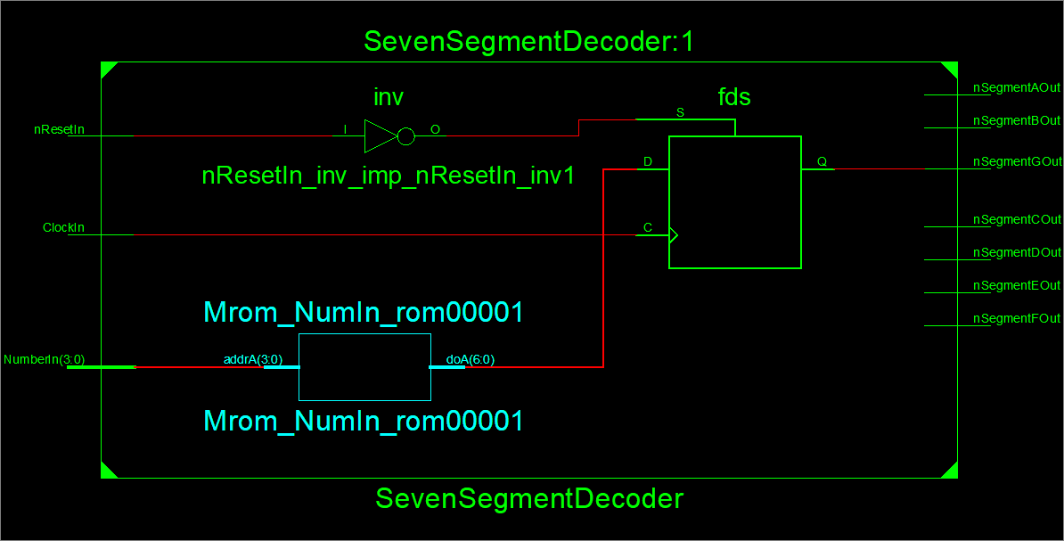
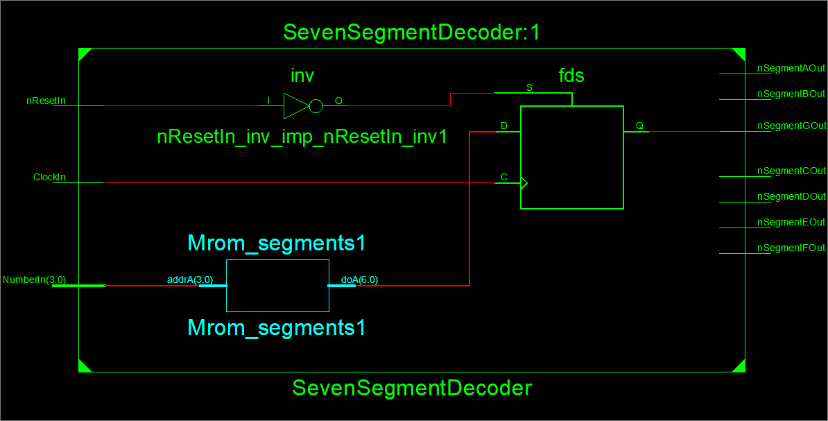
Attached files:

daniel__m wrote:
> There will be no benefit in terms of timing (it is the same netlist).

 In the pictures we see implementation same function of decoder : one
released by case statement other by if statement (Before optimisation by
development tools).

 Case statement implemented by set parallel LUTs with propagation delay
of one LUT.

 If statement implemented by set of sequence (consecutive) of 7 CELs
with propagation delay of 7 (or more) CELs (x 7).

  This is the different before optimisation by development tools.
 You don't know what will be after optimisation.

 Regards Alex.

 P.S.

 It's same implemented function but with different speed.
Alexander S. wrote:
> It's not only work, it's work more quickly than If ... elsif ... else
> statement and this purpose of using.
I proved that this statement is wrong in
https://embdev.net/topic/498163#6303923

Alexander S. wrote:
> In the pictures we see implementation same function of decoder : one
> released by case statement other by if statement
Of course there is a difference in sourcecode, then there must be a
difference in the direct RTL translation.

> It's same implemented function but with different speed.
At this point of the design (RTL schemtic) there is no "speed" involved
at all. Show an implementation schematic, then we discuss about timing.

> Before optimisation by development tools
Show a difference after optimization. Then we discuss further on. No
one can put a "unoptimized" design on a FPGA, because this kind of
"optimization" is only a reduction of logic like student do it with a
Karnaugh map. And before the K map a design is always "unoptimized". So
thats indeed no "optimization", but just the usual way of
implementation.

> You don't know what will be after optimisation.
How the toolchain implements my desgin doesn't matter at all. But I know
for sure that the timing will meet my constraints. Otherwise I will get
an error message.
And when this error message shows up, then I start seraching the
critical path with the STA tool. And then I will fix that path.
It IS really that simple.

And for such simple if-elsif-endif translations you will get always an
optimal implementation. Show one that doesn't result in an optimal
hardware in the bitstream, then we discuss further on.

Alexander, it seems like you have established your personal design rules
based on personal experience with an old fashioned toolchain not capable
of proper implementation and not able to use initial values.
But that was at the end of the 1900 or the early 2000s. Now we have 2020
and design style and the according rules have changed. The toolchain
programmers have done their job and you don't have to think one second
about such simple and obviuos translations.
Lothar M. wrote:

> But that was at the end of the 1900 or the early 2000s. Now we have 2020
> and design style and the according rules have changed.

But synthesis tools implement case and if statement such as 1000 years
before we see that on the pictures and optimisation tools not guaranteed
always realisation of optimisation.

 Regards Alex.
Lothar M. wrote:
>But I know for sure that the timing will meet my constraints. Otherwise I >will
get an error message.

 If you will get error message only after assembly full  design  (of
designers team) project , you will redesign your part and teams of
designers will wait that ?


 Regards Alex .
Lothar M. wrote:
>And when this error message shows up, then I start seraching the
>critical path with the STA tool. And then I will fix that path.


>It IS really that simple.

 For small design of single designer.

 Regards Alex.
Lothar M. wrote:
> In the pictures we see implementation same function of decoder : one
> released by case statement other by if statement

> Of course there is a difference in sourcecode, then there must be a


> difference in the direct RTL translation

 and propagation delay (speed).

 In one pictures propagation delay is propagation delay of one LUT

 In other pictures propagation delay is propagation delay of 7 CELLs (x
7).

 You think optimisation tools can repair that and propagation delay
always will be same ?

 Regards Alex.

P.S.
Preferred that design work without it optimisation by development tools.
So , after it optimisation it will be work with greater guarantee .
Attached files:
-

sseg_if_rtl.PNG
12 KB -

sseg_select_rtl.PNG
12 KB -

sseg_when_rtl.PNG
12 KB -

sseg_case_rtl.PNG
12 KB


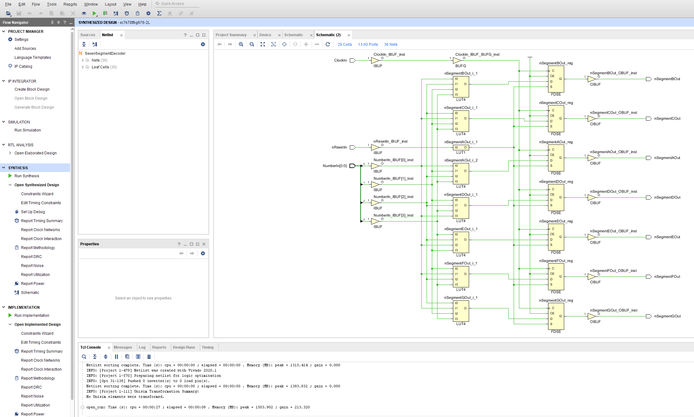
Alexander S. wrote:
> But synthesis tools implement case and if statement such as 1000 years
> before we see that on the pictures
Yes, we do.

> we see that on the pictures
When I feed the Xilinx ISE 14.7 with 4 different designs
(if/select/when/case) I always get the very same picture as RTL
schematic. All of them simply show a ROM. So obviously all of the
descriptions will lead directly to exactly the very same result in
hardware.

> and optimisation tools not guaranteed always realisation of optimisation.
This conclusion is fundamentally wrong. At least until you prove it.

Because even the translation from VHDL code to RTL schematic is a kind
of "optimization". Or do you see a "case" in the RTL schematic? No, you
don't. The "case" is "optimized" to a lookup table. Do you trust the
toolchain here, but not further on? If so: why?

> and optimisation tools not guaranteed always realisation of optimisation.
And of course nobody won't guarantee you anything. Even the synthesizer
may translate the "case" statements to the wrong LUT content.

Alexander S. wrote:
> Preferred that design work without it optimisation by development tools.
So, the only way will be to generate the bit stream manually. And even
for that you will need a K map. But you are not allowed to use that way
of "optimization".

Alexander, I'm finished here.
Sit on that little heap of sand and wait till the end comes...
Attached files:

Lothar M. wrote:
> The "case" is "optimized" to a lookup table.

The "case" is "optimized" to the set of parallel lookup tables.
The "if elsif else " is "optimized" to the set of consecutive CELLs
(LUTs).

 The optimisation tools can't change that architecture. You can't use
ROM for all "if elsif else " statment in your design : it will be set of
consecutive CELLs (or LUTs).

Sit on that little heap of sand and wait till the end comes...

 Regards Alex.

Good luck in your high speed design in the teams designers.
Attached files:
-

SBAv5c.png
89 KB -

SBAv5d.jpg
130 KB
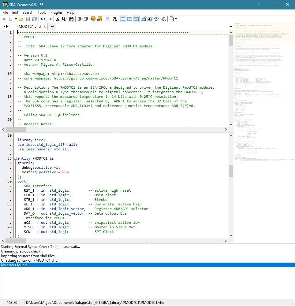

Other VHDL editor with editable templates SBA System Creator:
http://sba.accesus.com/software-tools/sba-creator

Also is easy write plugins to run external tools.

regards

MARC
Alexander S. wrote:
> The "case" is "optimized" to the set of parallel lookup tables.
> The "if elsif else " is "optimized" to the set of consecutive CELLs
> (LUTs).

No. What your pictures are showing is the elaborated Design. This is
simply what is written in HDL without optimization. It just shows what
the Toolchain thinks you described in HDL. But this is not FPGA specific
or optimized. In this View you can have and see individual Gates like
AND. But in the FPGA there are LUTs.

The Toolchain has to take your Logic like Gates and Registers and then
map this to the Hardware available. This is combined with optimization.
So it will combine many Gates for Example an put them together in a LUT.
Or a statemachine in BRAM.

To see what the toolchain created and is loaded to the FPGA you have to
look at the Schematic of the implemented or at least synthesized design.
Or to be more precise:

Your first two Images show the Logic after sythesis, but the last Image
"Lothar_M_Decoder_Implementation.PNG" shows the elaborated design.

Why are you doing this and compare synthesized vs. unsynthesized? This
in unfair to Mr. Miller.
Please log in before posting. Registration is free and takes only a minute.
Existing account
Do you have a Google/GoogleMail account? No registration required!
Log in with Google account
Log in with Google account
No account? Register here.