Hello everyone .

I have a project on VHDL . I have to create a 5 bit shift reg , with the
following options :

000 : Reset /
001 : Parallel loading /
002 : Right shift /
003 : Left shift /
004 : Circular right shift /
005 : Circular left shift /
006 : 1s' complement /
007 : 2s' complement

I have every module , but i can't create the final module , i don't know
it's structure . Any help ?

D flip flop : https://pastebin.com/Myj69R0L
Half adder : https://pastebin.com/AAYpA4br
Mux 8X1 : https://pastebin.com/w6r14wee
prescaler : https://pastebin.com/XH9Mtzyq

Code is attached too .
I have to use these components so i can have all the "options" that
final product needs to have .

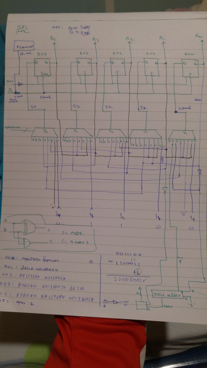
I have a schematic but unfortunately it is still a draft , and not
completed .
The schematic is wrong .

Black lines going upwards , were meant to connected on the inputs .

I will upload the right schematic later today , and now i started to
understand how to make it happen .
Could you describe what each of those do?

000 : Reset /
001 : Parallel loading /
002 : Right shift /
003 : Left shift /
004 : Circular right shift /
005 : Circular left shift /
006 : 1s' complement /
007 : 2s' complement

Reset is load with all zero?
Parallel load ok
Right,left shift ok but where is input and output?
Circular shift, ok, input = output?
1s and 2s complement?! Does this matter? Is is just a series of bits ...

Try to describe each "function" in HDL and then pack it in a case
structure.
> Reset is load with all zero?
Yes
> Right,left shift ok but where is input and output?
You get a 5 bit input an a standard output, and every time you select
what you want to do with input .
> Circular shift, ok, input = output?
yes
> Try to describe each "function" in HDL and then pack it in a case> structure.
I have to do it using different modules
- - - - - -
BTW , i think i made it working !
You give a 5 bit input and the number of the selection (what to do) and
it gives output based on them of course .
I have uploaded the file . Of course this one doesn't use the prescaler
, it's just for simulation .
Wow, lots of Errors, you did not even try to simulate.

But i fixed them ... and still it does not work as intended. Am i right
that with SEL = "010" it should shift right with every clock?
Sorry for the late reply .

I don't get any errors , only 2 warnings if i remember corectly.

Sel='010' shifts left every clock , circular .

Here are the final's programms options (sel) , sorry .


000 : Parallel loading /
001 : Right shift /
010 : Left shift /
011 : Circular right shift /
100 : Circular left shift /
101 : 1s' complement /
110: 2s' complement

Can you help me fix the errors you found ?


Thamnks a lot
Michael K. wrote:> I don't get any errors , only 2 warnings if i remember corectly.
I get errors for
I(5) =>not(INP(0)),
in port map.
and for
clear =>not(res),
and for
Sout =>sum2,
because Sout is not defined in half_adder.
But if it works for you every think seems to be fine.
I changed S to Sout in half-adder , to avoid problems .

I uploaded the files again (ignore prescaler that it is inside) , i
would really appreciate it if you test it and help me a little with the
test bench file (i can only check 1 input and 1 option (sel) per time) .
Thank you very much for your help .

It works OK from what i see in the simulation .

I will have to get the fpga (spartan 3) this coming week to test it , so
i'll probably need to figure out how to upload it to the fpga too (will
update here too) .

Thanks a lot Gustl and everyone else that helped with their answer !
Thank you! And yes, it is a hard long way :-)

So ... i think it is not working. Here pass many clockcycles while
nothing changes, no shifts or so.

HDLs like VHDL can be used even on a more abstract level. Ne need to
describe singe FlipFlops. A shift register with 5 bits can be written
as:

signal register: std_logic_vector(4 downto 0); --5 bits total
...
begin
...
register <= register(0) & register(4 downto 1); --circular right shift
register <= register(3 downto 0) & register(4); --circular left shift

And the MUX can be written as

if .... then
elsif ... then
endif;

or with the case statement.
Thanks . I'm new to all this so i'll have to learn a lot .

Check the file , for me the project you sent me works OK . EKS is the
output , and everytime it is as requested .
Really? I understand shift registers a bit different:

When it is in the state "shift right" the contend is shifted right one
step with every clock cycle. So in the waveform sel is 1 ("001") and
there are many clock cycles but is does not shift with each cycle.

It should look like
http://www.cse.psu.edu/~kxc104/class/cmpen297B/08f/hw/hw7/serialShift2.png
or the contend:

sel = "001"
it gehts loaded with "11000" and then it should shift:
"11000"
"01100"
"00110"
"00011"
...

But maybe we have different understanding and it is all right.
To be honest i don't know if it is requested to be in that way . But i
understand now what you mean .

Is it difficult to modify current project to work as you suggest ?

Thanks
Hm, the way you started is very educating, but not easy. Yes, you can
describe every single FlipFlop and MUX and half-adder, but you could use
the language constructs from VHDL instead. I don't know your constraints
if you must describe each element on its own.

I attached a waveform which shows what i guess it should show :-)

The register contains "11000"
Then res goes high for one clock
The register contains "00000"
Then sel goes to "001" and the registers loads the input "11000" again.

Then 3 clocks right shift:
"0110"
"00110"
"00011"

Then 3 clocks left shift:
"00110"
"01100"
"11000"

Then 6 clocks Circular right shift
"0110"
"00110"
"00011"
"10001"
"11000"
"01100"


Then 6 clocks Circular left shift
"11000"
"10001"
"00011"
"00110"
"01100"
"11000"

But i don't know what is meant by
1s' complement and 2s' complement. They are representation of numbers.
Should the shift register count or somethig like that? Or should the
contend be converted?

Edit:
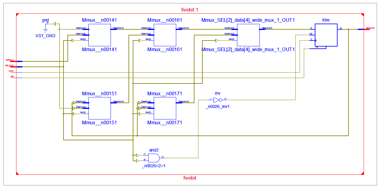
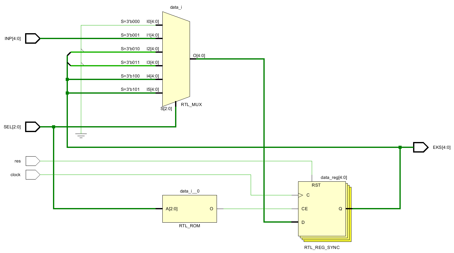
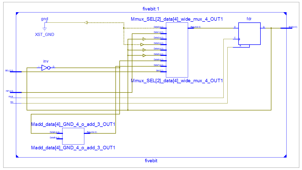
I attatched the schematic view from xilinx ise (the software you use)
and from the newer vivado (which does not support spartan FPGAs). Looks
like your hand-drawn schematic is very close to the schematic ise made
from my hdl code which is working. but on more intensive look not sooo
close. i recommend to write it in a more abstract way, not describing
instantiating single FFs and MUXes. Let the toolchain do that for you.
Just asked and you're totally right . It has to change every cycle.

Thing is i can't really figure out how to do it .

Btw , 1s complement is the opposite . for example , if you give 11001 it
should give 00110 and 2s complement is : 1s complement plus 1 (previous
example gives 00111).
OK, so ... i attatched the Testbench and a startingpoint for the
fivebit.vhd description.

The only data which is stored in this description are the bits in the
register:
The output is directly connected to the content of the register:
1
EKS<=data;
then we use a clocked process, so everything is triggered with the
rising edge of clock:
1
processbegin
2
waituntilrising_edge(clock);
3
.
4
.
5
.
6
endprocess;
The reset "res" is synchron with the clock, read as "if res = '1' and a
rising edge of clk happens" then the reset is executed. asynchron reset
should not be used in modern FPGAs.

After the reset there is the MUX which can be written as many
1
ifSEL="001"thendata<=whatever_you_like;
2
elsifSEL="010"thendata<=whatever_you_like;
3
elsedata<=whatever_you_like;
4
endif;
it can also be written like
1
caseSELis
2
when"001"=>data<=whatever_you_like;
3
when"010"=>data<=whatever_you_like;
4
whenothers=>data<=whatever_you_like;
5
endcase;
The "when others" case is mandatory. in the fivebit.vhd i used if ..
else description.

I wrote the first 4 entrys:
the rest is left for you. circular right/left shift is like normal
right/left shift but with the bit falling out at one end shifted in the
other end again.
I still don't really understand what should happen to the bits in the
register with 1s or 2s complement selected. And with normal right/left
shift this
1
elsifSEL="010"thendata<='0'&data(4downto1);
shifts right, and the leftmost bit is filled with '0'. Is this how it
shold be or should the leftmost bit be for example a new bit from the
input?
like data <= INP(0) & data(4 downto 1) or so ...
Gustl B. wrote:> OK, so ... i attatched the Testbench and a startingpoint for the> fivebit.vhd description.
Nice job, but I think it must be cleared whether those components from
the initial post MUST or CAN be used.
When they MUST be used then it is a fairly stupid exercise for
structural description from an old fashioned teacher (because in real
life nobody will instantiate a flipflop or a adder by using components
explicitly).
If they CAN be used, then i would kick then beside and do it like your
simple examples in less then 30 lines VHDL code.
Up to now for a pity it looks more like they MUST be used... :-/
Lothar is totally right (and i also wrote it):
Gustl B. wrote:> I don't know your constraints> if you must describe each element on its own.
Please ask your Teacher.
Because of cluelessness and lazyness i still would go the easy way.
Describe the logic in simple vhdl, look at the RTL view of your
toolchain (i posted a picture above somewhere) and then implement this
picture (= a working schematic) with the components you have to use.
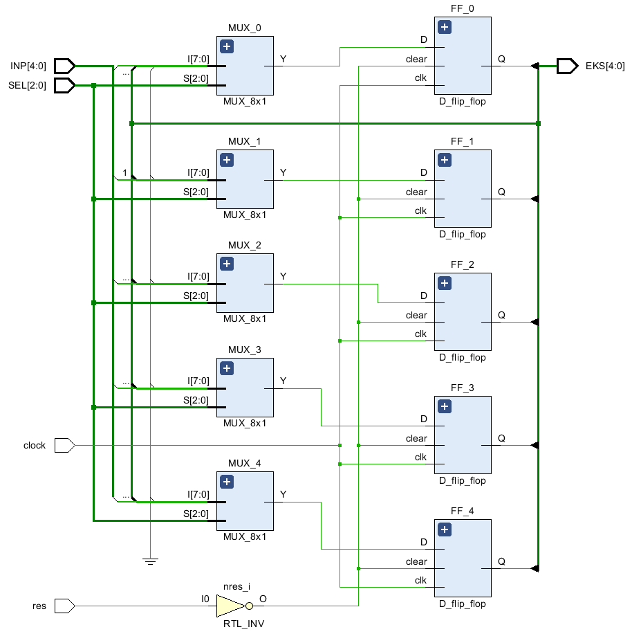
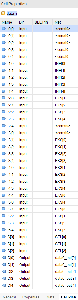
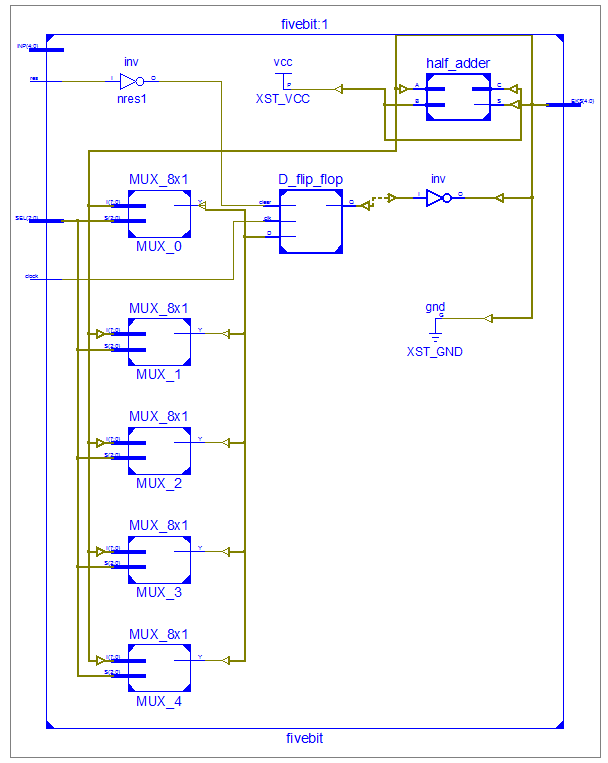
Wohoooo! It works (in simulation)! But ... it was tricky. Use the VIVADO
schematic because VIVADO uses the right MUXes. And then you have to dive
deep in vivado and get the details for all connections.

000 : Reset /
001 : Parallel loading /
002 : Right shift /
003 : Left shift /
004 : Circular right shift /
005 : Circular left shift /

can be implemented this way with 5 MUXes and 5 FFs and one inverter (for
res) because reset in your FlipFlop HDL has an active low clear.

I also attatched the mux.png it shows how the mux is connected in the
schematic_vivado.png it can be implemented as 5 independed muxes with
the mux HDL description you provided.

what i could not implement was the thing with 1s and 2s complement. i
understand what 2s complement is, but not how it should behave in the
shift register. the question is:

contend of the shift register is data(4 downto 0)
now SEL = "110" (6).
what should happen with every rising clock?
data <= ?
And what should happen if SEL = "111" (7)?
Gustl B. wrote:> contend of the shift register is data(4 downto 0)> now SEL = "110" (6).> what should happen with every rising clock?> data <= ?
i asked the same and i'm waiting for reply from my teacher .
> And what should happen if SEL = "111" (7)?
nothing .
-------
Can i do the process you mentioned in ISE ? Because i have to
Michael K. wrote:>> And what should happen if SEL = "111" (7)?>> nothing .
Souldn't this be the 2s complement thing?
1s complement is easy but for 2s complement you need an adder or more
complex logic.
My guess is that with SEL = 110 with every clock the content in the
register should be converted like 1s complement. and so with SEL = 111,
with every clock it should be converted in 2s complement.
Michael K. wrote:> Can i do the process you mentioned in ISE ? Because i have to
I don't know. i might be hard because ISE does not use 8-input MUXes in
the RTL schematic. the HDL is independent from ISE or VIVADO, so if you
once wrote the HDL files in vhdl you can use an simulate them with ISE
or VIVADO.
Here i only needed VIVADO to get the information about what is connected
to what.
Edit:
I just added the SEL = 110 and SEL = 111 cases as:
[vhdl] when "110" => data <= not data; --1s' complement
when others => data <= std_logic_vector(unsigned(not data) +1);
--2s' complement (SEL = "111")[vhdl]
and ... now ISE uses 8-input MUXes in the RTL schematic. Just like
VIVADO. In the waveform you can see that with SEL = 110 all bits in the
register are inverted with every clock and with SEL = 111 all bits are
inverted and 1 is added with every clock. But i don't know if this is
intended.
If this is ok, then you may use ISE, it looks good.
Gustl B. wrote:> Michael K. wrote:>>> And what should happen if SEL = "111" (7)?>>>> nothing .>> Souldn't this be the 2s complement thing?> 1s complement is easy but for 2s complement you need an adder or more> complex logic.> My guess is that with SEL = 110 with every clock the content in the> register should be converted like 1s complement. and so with SEL = 111,> with every clock it should be converted in 2s complement.
I was confused because in my project i had 7 options , and reset was
connected straight to tue flip flops . Yes if you use 000 option as
reset , 111 will be 2s complement .
I'll ask my teacher and/or an older student tomorrow if they have any
idea if it's possible to do it from my current project . I'll also have
to check the the last testbench file you uploaded earlier today .
Thanks again
I really appreciate your help !!

It seems and it really is easy that way , let's hope i can do it like
this (not really i guess :( ) .

More tomorrow (it's night here).

Thanks !
No Problem, i learn something too, good Night!

Edit:
And it works. Schematics attatched. But it was not easy to dig through
the very strange signal names in ISE. And it's very sag that neither
vivado nor ise show signal names in the schematic, you have to klick on
the lines. you also can't show busses as individual wires.
I think i finally made it !

My Diagram in post #6 has the solution ... In 000 option (parallel
transfer) you transfer the input to the output . Then EVERY time , you
give as input to the mux's from the output of option 000 (parallel
transfer) , and so every time it gets the output without the user doing
something . Basically to change input you have to give a new 5 bit input
and re-run 000 option .
Ok, very good! Respect! In Simulation are too few clock for circular
shifts, so you don't see if it shifts really circular. But this is easy
to fix in the Testbench.