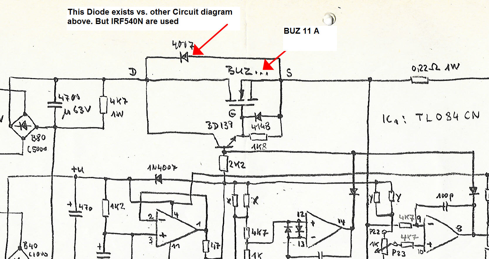
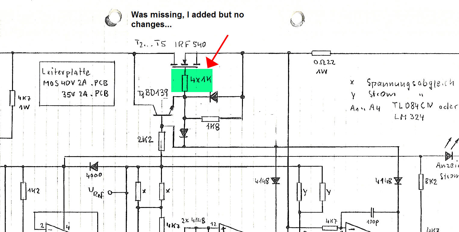
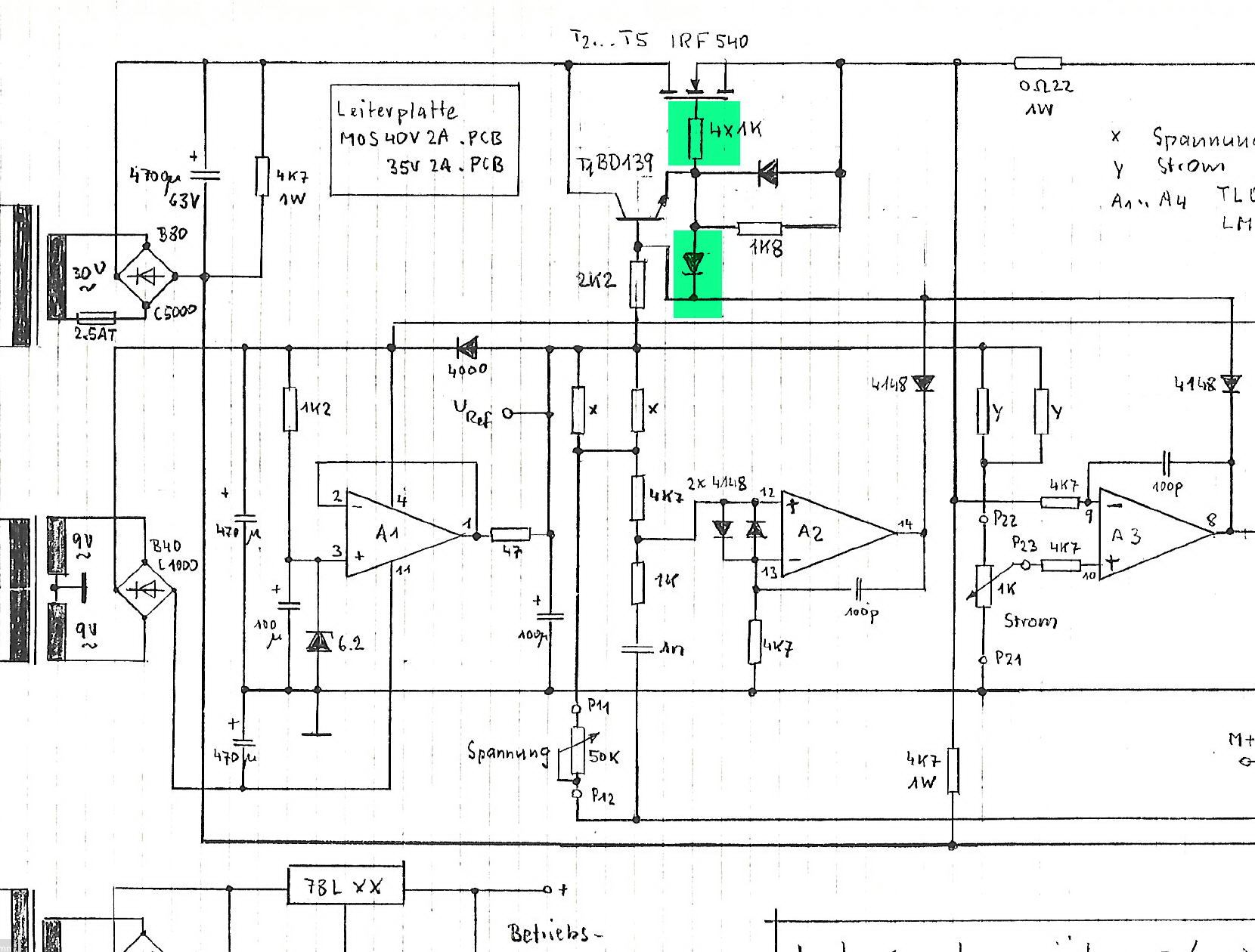
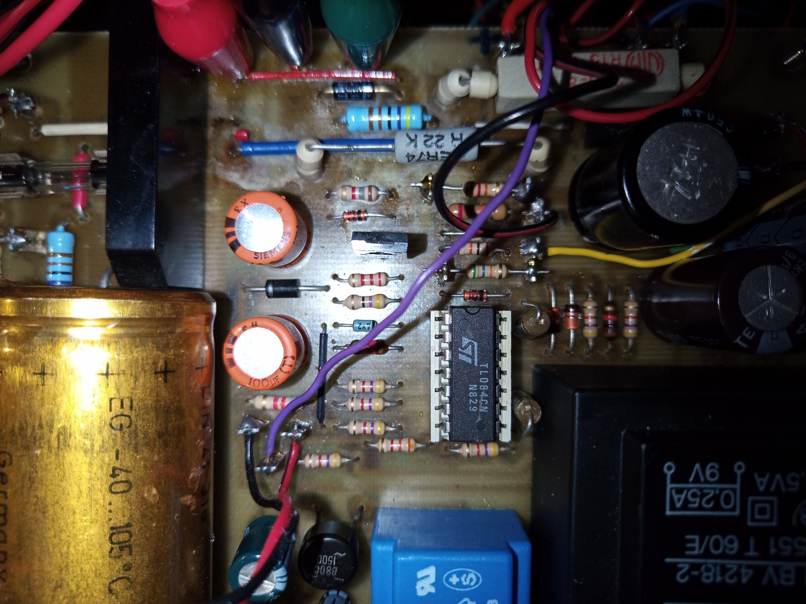
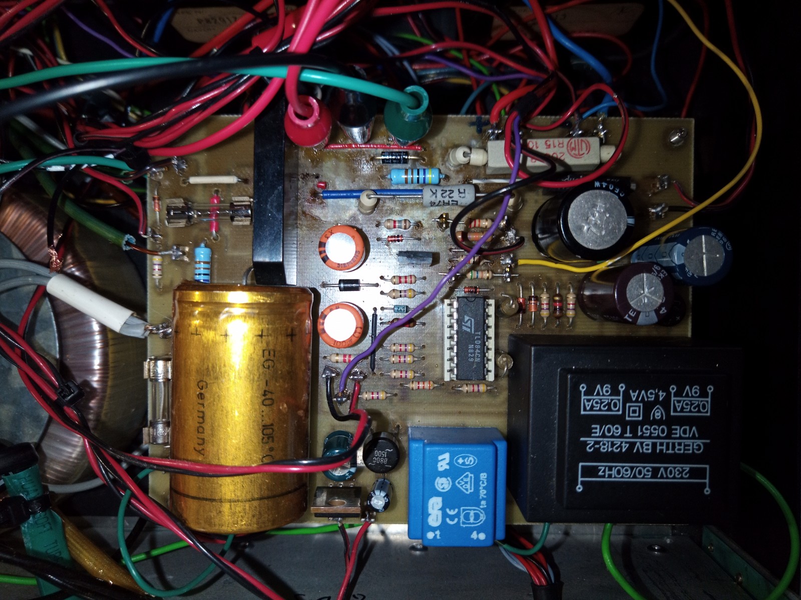

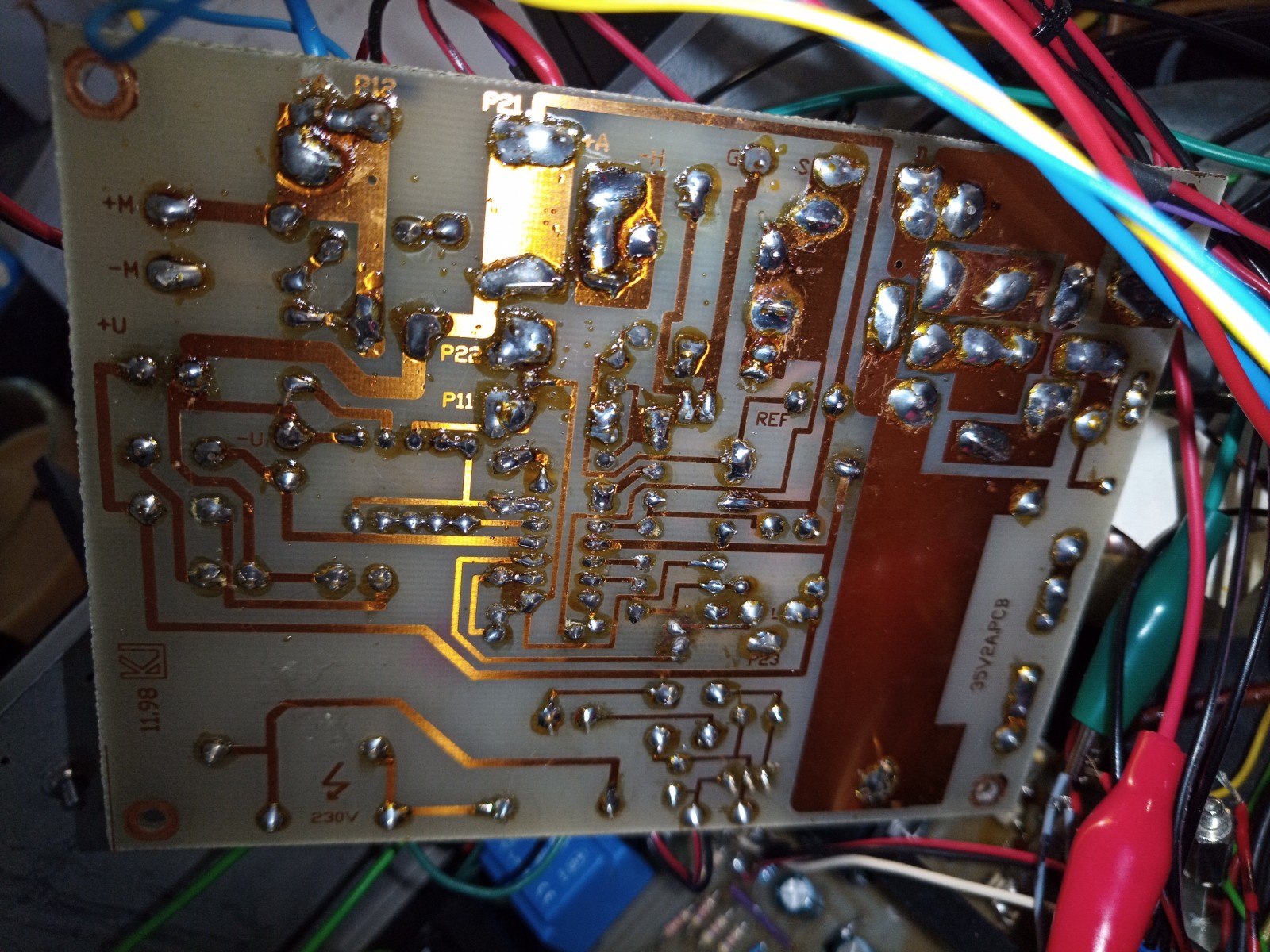

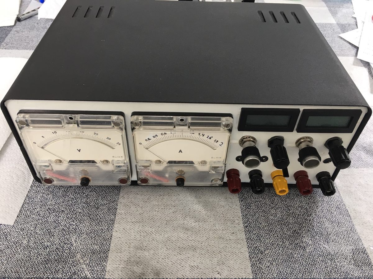
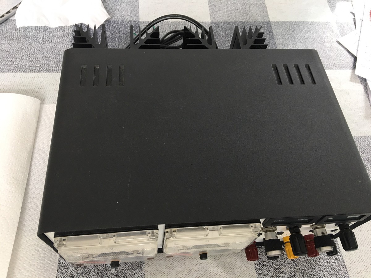
Hello to all here,

Since I restore and repair vintage transistor radios, radio recorders
and vintage hifi items myself, the need for a laboratory power supply
came up. Usual switch mode power supplies from China were unsuitable for
me, since these as you surely know disturb the SW, AM and LW reception
e.g. with a transistor radio massively. Therefore it had to be something
"linear". So I had bought a up to 95% finished „old“ 2 channel power
supply from an older guy who owned an electronics company here in
Germany. He told me, it was built by one of his employees (according to
him an electronics engineer) in the early 90s. It was built according to
a circuit diagram from the University of Frankfurt and the engineer
allegedly even built several devices of it. So he also handled me the
ciruit diagrams attached and additional 4 other, new  IRF 540N he still
did have. Much more he could not tell about the device.

The basic regulation of both boards (i.e. of both channels) works
perfectly and over the whole range. Also the current limitation is ok
and reacts well. But there are problems with the MOSFET. I have dealt
with them intensively and also researched. And so I also found some
videos on YouTube about paralleling MOSFETs. However, I am not an
electronic technician, but my main focus is rather the restoration. Even
if I made many self-construction devices in my young 20's, including PCB
creation "home brewed".

The parallel connection of the MOSFETs seems to be not without problems:
What is described in the internet in various (technical) places happens
also here with this power supply: The currents are distributed very
differently over the 4 MOSFETs. These are IRF 540N. During the (not very
long "endurance test" with 24V and just 1.2 Ampere already as my first
test one of these MOSFETs already broke down, the reason can be found
further down in the text ...I think. I have exchanged (repaired) this
one. Now it is so that e.g. with 2 running MOSFETs (connected as a test)
and 9V / 300mA (bulb) at first some 150/150 mA measured through both
MOSFETs. One of them quickly becomes much hotter and the current is
quickly distributed much more unequally (200/100 mA) between the two as
the temperature rises. With 2 bulbs connected, making i.e. 600 mA load,
this is even so that 400/200 mA is distributed between both 2/3 : 1/3
and the MOSFET with 200 mA even goes below 100 mA share of total load as
the temperature rises. So almost everything over the one MOSFET then
only runs. With all 4 MOSFETs connected, only 1 MOSFET gets hot at 600
mA, because all load runs completely over only this one MOSFET. The 2A
reading per channel can never be enough. This (from my opinion) also was
the reason the one MOSFET was destroyed with the 1,2A – all current did
flow over it

I made some tests: A resistor of 1K Ohm at the gate (like in the
schematic, "original" was not available) did not change anything. Also
connecting 2 or 4 trimmers (variable resistor, 4.7K set to 1K) in front
of the gate of each of the 2 or 4 MOSFETs with various "try adjustment"
did not change the current distribution.

Now you may have to select the MOSFETs a little bit, I had read this
where. Or I try the BUZ11A as MOSFETs instead of these IRF540N (these
are noted in the "hand-drawn" plan, but they are even more low power).
There are also minimal differences between the two schematics. The PCB
is the same as the hand drawn one, but with the IRF540N but without the
1K gate resistors which are marked on the "professional" schematic.

So my question would be primarily, if there is a fundamental design
error in the circuit? Which would mean, that it would be useless to try
to get the unequal load distribution under control. Or is it only badly
selected components (MOSFET) the problem. Or it makes sense to try to
use BUZ 11A MOSFET or to change or add something to the circuit. Before
I invest more time and money in the device, I wanted to make sure that
there is no basic circuit design error. Because otherwise I rebuild the
device with the good parts further used (housing, large toroidal
transformer etc.) with another circuit without MOSFET.

May bee you have some idea for what I can do more. I'm glad for any
tips.

Greeting Mathias
Attached files:
-

Infos.jpg
220 KB -

Missing_1K_Ohm_resistors.jpg
150 KB -

Variations_between_2_CD.jpg
370 KB -

inside1.jpeg
420 KB -

inside2.jpeg
430 KB -

inside3.jpeg
450 KB -

inside4.jpeg
460 KB -

inside5.jpeg
470 KB -

IMG_5199.JPG
230 KB -

IMG_5200.JPG
240 KB
Ad a small Value resistor in each source path before connecting them
together..
Magnoval wrote:
> Value resistor in each source path before connecting them
> together..

The temperature must goooood distributed of all MOSFETs T2...T5!
Mathias wrote:
> there is a fundamental design error in the circuit?

Yes.
It's a schematic of a bipolar power supply that simply replaced the NPN
by MOSFETs.
This will never work.
Neither the direct paralleling of MOSFETs without current distribution
resistors with about a voltage drop of UGSth at the full current a
MOSFET will have to hande is ok.
Nor the Gate-drive that is not symmetrical to charge and discharge the
gate.
And the whole signal response of the circuit is also not matched to the
different behaviour of the MOSFETs. Replace them with 2 2N3055 in
parallel with 0.22 ohms emitter resistor, and the power supply will
probably work right out of the box.

Or read: http://www.dse-faq.elektronik-kompendium.de/dse-faq.htm#F.9.1
and the chapter
http://www.dse-faq.elektronik-kompendium.de/dse-faq.htm#F.22.2
Hello, thank you very much for this information. To be honest, I was
afraid that something was simply designed together in an unprofessional
way. I think it would be a very good approach if this could be replaced
by normal power transistors. Actually I would prefer that. How should I
connect it concretely? Would there be a diagram? That would help me a
lot.
Would it be possible to use an alternative for 4 power transistors in
the TO220 package? Because these holes would already be there. But
otherwise I can install the 2 x 3055. There are 2 large heat sinks.
Mathias wrote:
> Would it be possible to use an alternative for 4 power transistors in
> the TO220 package?

TIP31 od BD241 will do the job.
Mathias wrote:
> Would there be a diagram? That would help me a
> lot.

There is probably no need for that, as the change is quite simple. The
BD139 already provides enough current to drive a 2N3055 or two of them
(you could also use BD130 or 2N3771-3773).
Replace the 1k resistor at the gate with a link. Connect the Collector
(case) of the 2N3055 to where the Drain was connected (rectifier
output). Connect the Base to the emitter of the BD139. Connect the
Emitter of the 2N3055 to where the Source was. If more than one 2N3055
is used , wire a 0.22Ohm/5W resistor in series of Emitters.
1 | from rectifier to PS output |
2 | >----+----------\___/--|===|--+ |
3 | | C E 0.22 | |
4 | +----------\___/--|===|--+----> |
5 | C E |
6 | |
7 | Tie bases together and connect them to emitter of BD139 |
Another power transistor would be BD249 in the TO3P package.
Hello matzetronics,

I'm going to rebuild it that way now.

Thanks you very much!
Vielen Dank!

Mathias
Mathias wrote:
> Would it be possible to use an alternative for 4 power transistors in
> the TO220 package?

The power supply is 30V/2A and needs to dissipate about 80 Watts.
A single TO3 insulated on a good heat sink may dissipate 80W (not the
115 a 2N3055 is advertised, that requires water cooling)
A single TO220 insulated on a good heat sink may only dissipate about
40W.

But why do we recommend two 2N3055 (not a single 2N3772 as they have a
terrible hFE current amplification) ?

Because the heat sink may be much smaller if 2 are used in parallel
allowing for cheaper construction. So you will have to use 4 in TO220 to
get the same benefit. Clamp them on a heat sink, not using the screw on
the tab as this will bend the metal tab away from the heat sink).

Each of them will carry only 0.5A, and should get about 0.5V on emitter
resistor, so 1 ohms should be used and may replace the 0.22 resistor in
the original. BD243B or C should do, or TIP41B or C.

> Because these holes would already be there.

Each of them does require a resistor in the emitter wire.

If you add more transistors in parallel, this will not require more
drive current and a larger drive transistor, as the output current
remains the same and hFE will not get worse.

A good construction will calculate the allowable heat sink temperature
that the transistors can survive at full load and place a thermo switch
on the heat sink to prevent damage on hot days or bad ventilation
(overcurrent may not happen as this is limited in a lab supply).
Hello MaWin,

thanks! This is also a very suitable solution with the 4 TIP41C. As it
does not need to drill additions holes on the heat sink. I can then use
the existing. To correct understand: Does it then need 4 x 1 ohms
resistors for each ones emitter, or 4x 0,22 ohms or only replace the
existing 0,22 ohms against a 1 ohms resistor (how many watts)? The 4 x
TIP41C are then paralleled like in the sample with the 2N3055 above?
Mathias wrote:
> Does it then need 4 x 1 ohms
> resistors for each ones emitter, or 4x 0,22 ohms or only replace the
> existing 0,22 ohms against a 1 ohms resistor (how many watts)?

Strike a happy medium and use 0.47 ohms, 0.5 W is sufficent.


> The 4 x
> TIP41C are then paralleled like in the sample with the 2N3055 above?

Exactly.
Mathias wrote:
> Does it then need 4 x 1 ohms resistors for each ones emitter, or 4x 0,22
> ohms or only replace the existing 0,22 ohms against a 1 ohms resistor
> (how many watts)? The 4 x TIP41C are then paralleled like in the sample
> with the 2N3055 above?

As the supply needs a 0.22 Ohm measuring shunt for the current that
increases its output impedance, it is not neccessary to increase that by
additional emitter resistors.
Just use them to replace the 0.22 ohm shunt.
4 parallel resistors to get 0.22 Ohm would need to have 0.88 ohm. As
they are not available I said 1 ohm (at 0.5A they only need to have
0.25W so the usual 0.6W metal film will do fine).
Then either connect a single emitter to the opamp below, or sum up all 4
emitter lines using 1k resistors, to get to the opamp. The latter one
measures more exactly if the summing resistors have 1% and not 10%
tolerance. With 4 x 0.82 ohms you are nearer at the specs, but you
probably have to buy them from Mouser. I doubt that Reichelt will stock
0.82 ohm 1% metal film.
1 | --+--CBE--+-----------1R--+-- out |
2 | | | | |
3 | +--CBE--(--+--------1R--+ |
4 | | | | | |
5 | +--CBE--(--(--+----1R--+ |
6 | | | | | | |
7 | +--CBE--(--(--(--+--1R--+ |
8 | | | | | |
9 | 1k 1k 1k 1k |
10 | | | | | |
11 | +--+--+--+-- opamp |
As a 4k7 resistor as  load is fitted to the joined source connectikn,
and you have 4 emitters now that are not joined, we need 4 18k resistors
to replace this.


Your circuit is a copy of
https://www.mikrocontroller.net/attachment/129845/0_35v_3a_labor_netzgeraet_elektor82_773.pdf

Only with non-working MOSFET and a poorer reference.
Hello, MaWin, thanks a lot! Could you please attached the PDF again it
states is not existing attachment, even in logged in status.
I could get 0,82 Ohms 1W but with 2% instead 1% from Reichelt. Will this
fit?
... but (?) should one or all 4 emitters get connected direct to the
opamp, not to the BD139?
Mathias wrote:
> but (?) should one or all 4 emitters get connected direct to the
> opamp, not to the BD139?

Neither this nor that. Have a look at the Elektro design. There is no
connection between the emitters of the power transistors to the BD139.
Don't get confused. The Opamp comes later and is designed to measure the
current across the shunt resistor.

MaWin posted a shortcut where the equalizing resistors provide the
current measurement as well as equalizing, but your original desing uses
a dedicated resistor for this (the 0R22 in the output rail) and theres
no need to change that. The equalizing resistors can well be seperated
from this function.
matzetronics wrote:
> Have a look at the Elektro design

that should write 'Elektor design' of course
A little additional note:
The IRF540N is a modernized successor where they could get the same
switching performance out of a smaller die than the original IRF540
without "N"
In analog mode it breaks at lower power

If you really want to go with MOSFETs i suggest something like the
IRF250
A-Freak wrote:
> If you really want to go with MOSFETs i suggest something like the
> IRF250

Note that MOSFets in this kind of circuit are still one of the wrongest
things one could do. MOSFets have no fixed relation between Source- and
Gatevoltage, which is essential in a follower configuration used in this
power supply. Instead the relation is subject to large variations. This
even  differs from item to item.
MOSFets used as sourcefollowers are in most cases a wrong choice.

A bipolar transistor on the contrary has a fixed voltage of approx. 0.6V
between Base and Emitter which also makes it possible to connect them in
parallel as (emitter-)followers without much effort. Best results are
achieved with items from the same charge, if this is not possible one
can use the equalizer resistors as described in this thread.
Mathias wrote:
> Hello, MaWin, thanks a lot! Could you please attached the PDF
> again it states is not existing attachment, even in logged in status.

That's sad, maybe they deleted it for copyright infringement.
But there was already help.
A (very!) long time ago I have developed a regulated power supply using
MOSFET (aka BUZ...).
In order to balance the currents, I have made a circuit using LM324,
that simply mirrors the source current of MOSFET 1 to MOSFET 2-4. The
control circuit only controls MOSFET1.
Each OpAmp compares the shunt voltage of MOSFET1 and sets the one of its
own MOSFET identical. (sorry for poetry instead of schematic!)

This has worked well. All Currents were identical, so was the power
dissipation. Not sure about the dynamical response. Those days I did not
care too much...
Please log in before posting. Registration is free and takes only a minute.
Existing account
Do you have a Google/GoogleMail account? No registration required!
Log in with Google account
Log in with Google account
No account? Register here.