How do i move the pads(each row of 4) of PCA8565 closer together in
EAGLE ?

PCA8565(real time clock) has a guage block(HE) of 4.7mm -5.1mm. The pads
on PCB has a distance of 4.65mm. This is has  been an issue in machine
assembly. NXP identifies components as TSSOP8 which is incorrect.

EAGLE identifies IC libraray files name as 00_ICs which i dont find in
C:\EAGLE 9.5.2\cache\lbr location ?

Thanks in advance for the help
- open library in editor
- show all layers
- mark all pads in a row, plus line of body, pin one mark,
cream/stop/other stuff eventually drawn there
- move
- save
- right click library in main window
- select "update"
- board is changed
- done
eagleuser wrote:
> - open library in editor
> - show all layers
> - mark all pads in a row, plus line of body, pin one mark,
> cream/stop/other stuff eventually drawn there
> - move
> - save
> - right click library in main window
> - select "update"
> - board is changed
> - done

HI, thanks for suggestion. But i have library file name 00_IC1 which
does not exist. I found NXP library file with PC8565. But different pin
setup. 5 pin on left,3 pin on right.

But the for IC on board have 4 pads on each side.
Ah, so you have a layout from someone else, and he used libs you don't
have?

The path to the lib is not necessary, the main window has a folder
"lbraries" that points to wherever you said in the settings, and that is
where all lbr files should be.
But if that is not your own design it's easier to just make one.
If you have a datasheet with mechanical drawing just go new/library and
make the chip yourself.
- make new package
- set pads
- name them 1,2,3 etc
- add placement drawing in 21
- add >Name in 25
- add >Value in 27
- make new symbol
- a rectangle and a bunch on pins
- name the pins like the signal
- make a new device
- add symbol
- add package
- connect properly
- save
- add to schematics/board
- check

If you need to correct something, you can.
Just "update" in main window after saving changes in lib editor and you
can see what changes.

Older versions had an ULP to export the parts used in the drawings into
new libraries so you could change and update unknown/missing lbrs by
mimicking them.
No idea if 9.5 still has this.
Attached files:
-

3D_package.PNG
36 KB
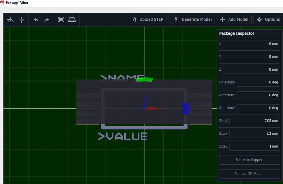
eagleuser wrote:
> Ah, so you have a layout from someone else, and he used libs you don't
> have?
>
> The path to the lib is not necessary, the main window has a folder
> "lbraries" that points to wherever you said in the settings, and that is
> where all lbr files should be.
> But if that is not your own design it's easier to just make one.
> If you have a datasheet with mechanical drawing just go new/library and
> make the chip yourself.
...........................................

Hi, Since customized old library file is deleted. I have generated 3d
package model. Can i change pad size using this model. Attached is
scrrenshot of 3d package editor.
Why make complex when simple will do?

I don't know anything about the 3D editor, that's useless for me.
Just use the normal lib editor, add pads and lines like stated above and
you could make your own part in like 5 minutes.
Attached files:
-

Supply_and_ground_plane.PNG
87 KB -

IC_pad_DRC.PNG
61 KB
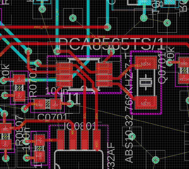
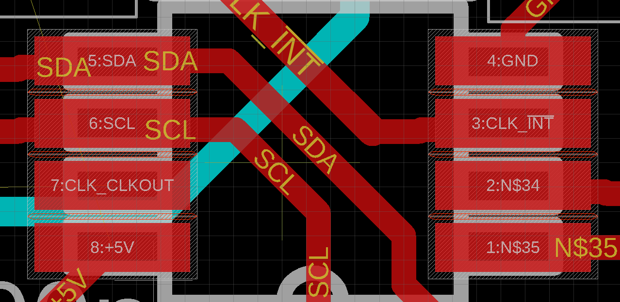
Hi,

I have replaced a package on layout. But now all ground and supply lines
are disturbed. PFA of image supply and grnd lines disturbed. Should i
make a ground and supply plane again.

I tried connecting from PAD to VIA of 1-16 layered with ground on 3
layer.


Also in other image does closer pad size make problem in DRC. i can see
red lines.

Thanks in advance
You either need to adjust DRC rules to what your manufacturer can do,
then if you still have errors you have problems because the board is not
doable by him, you need to find another one.
Or you just did the chip design wrong...
I'd say the latter, the pads are way too close i think. Also, there
always should be a tstop line betwen the pads.

It seems your chip center is not centered, also the grid is a bit
coarse, hence the wiggly lines.
Always start from the pad (Eagle always comes out straight) and connect
to a grid point slightly above or below center of pad. That way you
always get a clean 45° angle and straight lines.

Rahul R. wrote:
> But now all ground and supply lines
> are disturbed.

What do you mean? The wiggly lines?
>
> What do you mean? The wiggly lines?

Yes, wiggly lines. when i replace old package with new one and connect
to ground and supply vias, It shows wiggly lines(all other connections
related to supply and grnd  it - routing lines disturbed showing more
DRC errors)

how do i make this yellow lines related to suppy and ground go away ?
Ah, you mean the yellow rubberbands....
Those are the unrouted connections, maybe because the polygons for GND
and such were ripped up.
Just ratsnest and the polygons will reappear.
Look in the status line after ratsnest if there are some signals left
you need to route manually.

BTW, this is a pretty basic function of Eagle, it seems you need a bit
of practice, and a good read of some tutorials...

I refered to the traces like "clk_int", that comes out the pad and steps
some down, then disappears to the top left.
Same is for SDA, SCL and the 2 traces to the quartz.
This looks just ugly to me.
Please log in before posting. Registration is free and takes only a minute.
Existing account
Do you have a Google/GoogleMail account? No registration required!
Log in with Google account
Log in with Google account
No account? Register here.