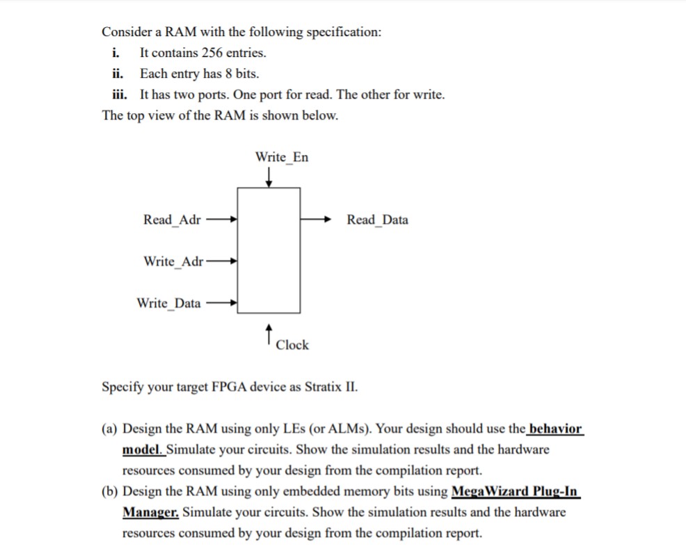
Do someone know how to code this program ? Problem(a)and(b).
They'll be compiled in quartus .
Attached files:
-

_20191219_175530.JPG
78 KB
VHDL problem for help wrote:
> Do someone know how to code this program ?
For sure. It isn't that difficult.

But your teachers intention is, that you do your homework on your own.
So lets try it that way: you start with something and then with
particular problems maybe someone starts to help you.
Lothar M. wrote:
> But your teachers intention is, that you do your homework on your own.

But let us guess: There is no time for that. It must be finished
tomorrow, right?
LIBRARY ieee;
USE ieee.std_logic_1164.all;

LIBRARY altera_mf;
USE altera_mf.all;

ENTITY RAM_2PORT IS
PORT
(
  readaddress    : IN STD_LOGIC_VECTOR (7 DOWNTO 0);
  writeaddress          : IN STD_LOGIC_VECTOR (7 DOWNTO 0);
  writedata    : IN STD_LOGIC_VECTOR (7 DOWNTO 0);
  readdata    : OUT STD_LOGIC_VECTOR (7 DOWNTO 0);
  en      : IN STD_LOGIC  := '1';
  clock      : IN STD_LOGIC
);
END RAM_2PORT;

ARCHITECTURE SYN OF ram_2port IS
  SIGNAL sub_wire0  : STD_LOGIC_VECTOR (7 DOWNTO 0);

  COMPONENT altsyncram
  GENERIC (
    address_aclr_a  : STRING;
    address_aclr_b  : STRING;
    address_reg_b  : STRING;
    indata_aclr_a  : STRING;
    intended_device_family  : STRING;
    lpm_type  : STRING;
    numwords_a  : NATURAL;
    numwords_b  : NATURAL;
    operation_mode  : STRING;
    outdata_aclr_b  : STRING;
    outdata_reg_b  : STRING;
    power_up_uninitialized  : STRING;
    read_during_write_mode_mixed_ports: STRING;
    widthad_a : NATURAL;
    widthad_b : NATURAL;
    width_a   : NATURAL;
    width_b   : NATURAL;
    width_byteena_a   : NATURAL;
    wrcontrol_aclr_a : STRING
  );
  PORT (
      wren_a    : IN STD_LOGIC ;
      clock0    : IN STD_LOGIC ;
      address_a  : IN STD_LOGIC_VECTOR (7 DOWNTO 0);
      address_b  : IN STD_LOGIC_VECTOR (7 DOWNTO 0);
      q_b  : OUT STD_LOGIC_VECTOR (7 DOWNTO 0);
      data_a    : IN STD_LOGIC_VECTOR (7 DOWNTO 0)
  );
  END COMPONENT;

BEGIN
  readdata <= sub_wire0(7 DOWNTO 0);

  altsyncram_component : altsyncram
  GENERIC MAP (
    address_aclr_a   => "NONE",
    address_aclr_b   => "NONE",
    address_reg_b   => "CLOCK0",
    indata_aclr_a   => "NONE",
    intended_device_family => "Stratix",
    lpm_type   => "altsyncram",
    numwords_a   => 256,
    numwords_b   => 256,
    operation_mode   => "DUAL_PORT",
    outdata_aclr_b   => "NONE",
    outdata_reg_b   => "UNREGISTERED",
    power_up_uninitialized => "FALSE",
    read_during_write_mode_mixed_ports => "DONT_CARE",
    widthad_a   => 8,
    widthad_b   => 8,
    width_a   => 8,
    width_b   => 8,
    width_byteena_a  => 1,
    wrcontrol_aclr_a => "NONE"
  )
  PORT MAP (
    wren_a => en,
    clock0 => clock,
    address_a => writeaddress,
    address_b => readaddress,
    data_a => writedata,
    q_b => sub_wire0
  );
END SYN;

sorry to bother you , can you tell me what I write is true or false ?
questioner wrote:
> is true or false

Depends. If the simulation results match the intended function, then it
is true. Otherwise, it is false. Without simulation, it is undefined.
Please log in before posting. Registration is free and takes only a minute.
Existing account
Do you have a Google/GoogleMail account? No registration required!
Log in with Google account
Log in with Google account
No account? Register here.