Hi there!

Last time has been worked a lot with my Arduino Nano clone. I has a
EAGLE 9 prototyping environment installed, so I have edited those files
in this workspace.

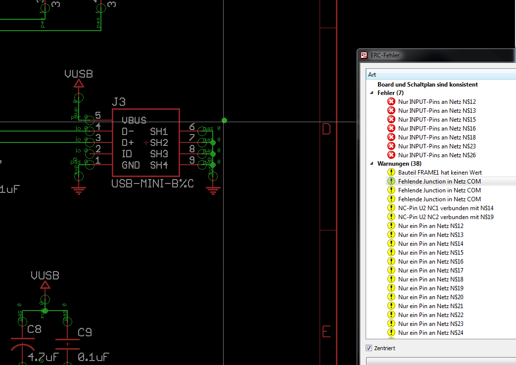
When I try to connect .brd with .sch, there is a lot of errors becomes
visible and I have no idea how to fix them.

Can't figure out this problem.

Any help is much appreciated!
Sorry, can't figure out how to change language in EAGLE. Just tried to
search, but nothing found. So, there is an image, but in Russian:

https://imgur.com/a/D0OjgEW

It is a "Consistency errors", like "Part U$36 not found in the board"
and
"Only INPUT pins on circuit..."
Mihail P. wrote:> like "Part U$36 not found in the board"
Is there a part U$36 in the board?
Mihail Podivilov wrote:> When I try to connect .brd with .sch,
Why and how did you split them?
You learned a important thing: never edit a *.brd without having opened
the corresponding *.sch!
It is too difficult for me to understand what is the U$36 part in the
circuit. I just modified the existing .brd / .sch, presented by
gravitech.us (original .sch & .brd atttached to this message in zipped
archive).

Can you help me to figure out what is the problem? When I try to edit
original .sch/.brd, there is also those errors are apperas, even if I
don't modified nothing.

Thanks!
Mihail Podivilov wrote:> Can't figure out this problem.
Simply delete the Logo in your .sch and you are done. Then keep in mind,
to work with projects and always open .sch AND .brd when you are working
with Eagle. So Eagle can hold both files in a consistent state, that
means, that there are no substantial differences between them. You had
inserted some "logo" in your Schematics and this got the number U$36.
W.S.
Thanks, it worked.

But I still have a lot of errors (like a "Only INPUT pins on circuit
N$12", "Only INPUT pins on circuit N$13", etc.
And a lot of warnings, such as "NC pin U2 NC1 connected to N$14", "Only
one pin in circuit N$27", etc.

What should I do right now? Thanks!
Mihail P. wrote:> What should I do right now? Thanks!
Ignore them, the designer uses maybe testpoints instead of pins so eagle
sees only one connection in the net. Additional there are only inputs on
this nets.
Others are missing junctions, you can add them with the junction
command.
Welp. Thanks!

Another one question is how to order assembly of this PCB? I heard about
multiple sites where I can do that, but help me to choose the right way
in my situation. I need to assembly up to 5 prototypes of them, so where
can I find the site to simply provide electrical scheme (.sch) and board
(.brd), then get a my produced board?
HyperMario wrote:> Others are missing junctions, you can add them with the junction command.
Can you give me an example how can I do this in proper way?
Mihail P. wrote:> Can you give me an example how can I do this in proper way?
Type JUN and put the green dot on the junctions where eagle claims the
missung junction
HyperMario wrote:> Type JUN and put the green dot on the junctions where eagle claims the> missung junction
Ok, done that. So, there are still 35 ERC warnings...
Mihail P. wrote:> Ok, done that. So, there are still 35 ERC warnings...
There are all OK.
The warnings are mostly different supply name between net and pin.
That's quite normal.
The errors depends on the designers intention to explicitly show that
unconnected pins means unconnected pins. He made a NC (not connected)
device to show that. Good idea i think.
HyperMario wrote:> Maybe it's easier to buy a nano directly.
Sure, but I want to understand how prototyping and final production take
place. :)
As a programmer, I also want to create special software to ease the
programming learning in our college.
Mihail P. wrote:> Sure, but I want to understand how prototyping and final production take> place. :)
Maybe you should consider a manufacturer where you get the stencil too.
Using solder cream (and a pizza reflow oven) is way nearer SMD
production than using a solder iron.
Hey, just figured out that jlcpcb.com is what I need. I has generated
gerber files (CAM data), but I want a real working prototype, not only
the PCB. I don't need to solder myself :)
Isn't .sch file is intended for data specification, such as AVR chip
info and same? I want to assembly a board with all components on them,
not only the board to solder later.
Mihail P. wrote:> I want to assembly a board with all components on them,> not only the board to solder later.
The pcb manufacturer needs the .brd file (or gerber and drill file).
Gerber is - let's say - not easy and error prone. You always have to
check with a viewer before production.
Manufacturing a complete board requires a BOM (bill of material).
Normally you have to specify all parts (except standard like resisitors)
with a unique MPN (manufacturer product number).
Just ordered 10 pcs of PCB prototypes. Good luck to me!
Will try to find somebody who can assembly the details in my country :)

And, as always, thanks!
Mihail P. wrote:> I has ATMEGA168-20AU specified in> .sch file (and such). Is it not enough?
The schematicic holds the information, I dont know if it's complete
You can build the BOM with the "run bom" command
Due to this design
https://www.rs-online.com/designspark/reference-design-of-arduino-nano-3-0
it's an ATMEGA328P-AU, there is the rest of the BOM too and RS has
branches in several countries
Mihail P. wrote:> But I still have a lot of errors (like a "Only INPUT pins on circuit> N$12", "Only INPUT pins on circuit N$13", etc.>> What should I do right now? Thanks!
You always should understand the schematics and how it is intended to
work.
When you have only inputs on a net, then WHO drives this net? Did you
forget to connect it to the output of a chip?
Messages like "Pin V+ connected to Vcc" or so are usually neglible, but
check them carefully and decide by yourself, if this is OK.
A bit more harmful are situations, where suppy-pins of some chips are
not directly shown in the schematics. Best example is a SN7400 (4
nands). Placing it in the schematics you will get all 4 gates, but the
supply connectiosn GND and VCC are usually hidden and automatically
connected to the rails GND and VCC - if they exist! So the better way
is, to invoke those supply items with the invoke function and connect
them by yourself to that rails you want them to be connected. The ERC
can halp you to detect design failures of such kinds, so do not IGNORE
them, but rather check them, if they are neglible or not.
W.S.