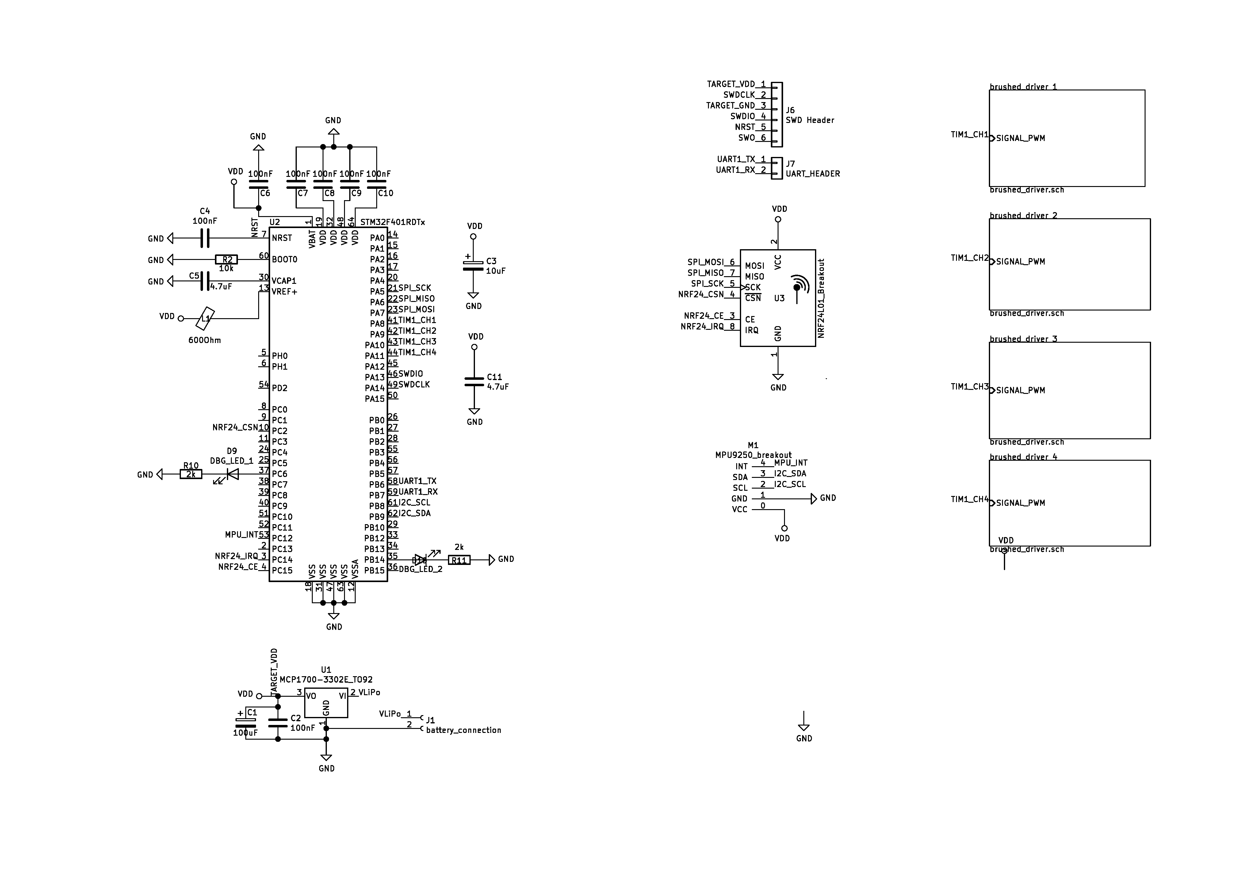
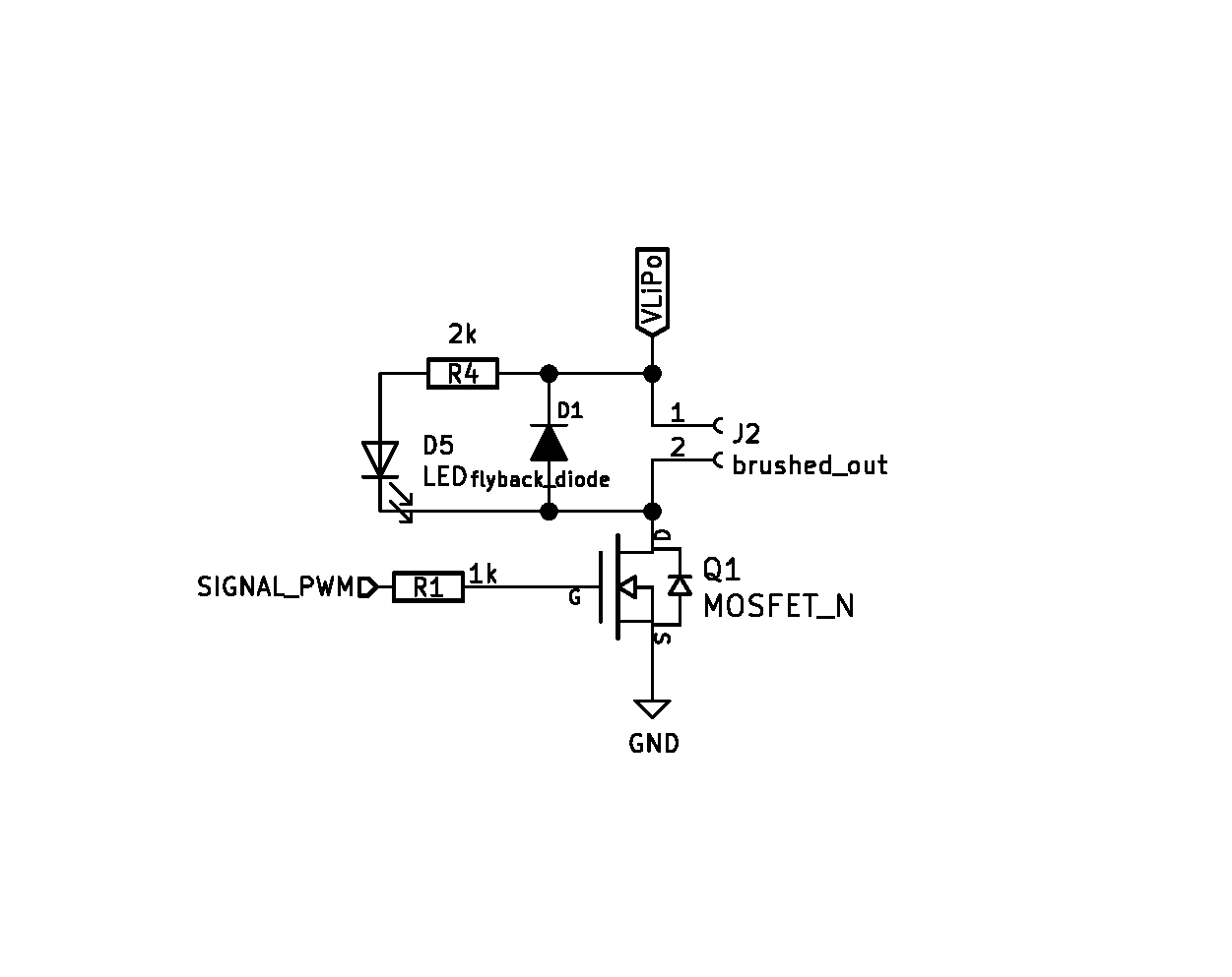
Hello,
I am trying to design a circuit for the STM32F401RDTx. I proceed as per
the datasheet, Application Note 4488 from ST, and Carmen Noviellos
"Mastering STM32" , but I don't find it simple at all right now and have
a few questions. I have attached the current state.

Firstly: how does the supply look? I have a LiPo that ranges 3.2V to
4.1V, and a MCP1700 3.3V LDO regulator with 2 caps that supplies VDD
with 3.3V. Does this suffice?

Moreover, I am not sure about the decoupling of the supply. I have
connected every VDD pin to GND via a 100nF cap. VBAT also, but should I
touch that at all? It goes to VDD at the moment.

What makes all this confusing is that even in the corresponding
application note for the processor, VCAP1, VCAP2, VREF+, VBAT, VDDA...
are mentioned but my LQFP-64 package only has VREF+, VCAP1, VDD, and
VBAT. For example, I do not know if I need the ferrite bead that
Noviello uses in the book between VDD and AVDD (yet another name for
VDDA (?)...), because I do not have a VDDA net.

Also, I chose 0805 for now, which I previously soldered using the hot
air station. But would it be beneficial for EMI to go smaller?

Sorry if all this comes across as a bit disoriented, maybe this is a bit
more than I can chew, but I want to try.
Attached files:
-

pcbQuad-page1.png
46 KB -

pcbQuad-page2.png
6.8 KB
The ldo has 0.178V drop voltage.

Define vcc to be 3.0 V and you're ok. Check that all components can
handle this within the defined operation range.
Use a ferite bed if you want to use the ADC and another capacitor.

Add also 1uF to the supply output. Bigger capacitor to the input.

All supply and grounds have to be connected.

Connect also JTAG/SWD.

The schematic is not showing the power supply as far as I can see.

The resistor size do no matter. The smaller capacitor are better for
emc/efficiency if you use short traces to the relevant supply pin. 100nF
is typically ok for such an MCU. 0805 ok, from my experience with an
lpc1768/9. One cap for each supply pin. Connect also the next/matching
ground near to this cap. The supply should first see the cap and then
the pin of the MCU.

Connect vcap with a capacitor as in the datasheet 4.7uF.

If you don't use vdda/adc treat it as vdd and connect it.


Connect all power pins. Connect vbat to 3V if you don't have a battery,
treat it same as any other supply pin.

Pins which are not available in your package can be ignored.


Kind Regards
 Thorsten
> Add also 1uF to the supply output. Bigger capacitor to the input.

I already have 4.7uF and 10uF (directly right of the uC in the attached
schematic). Should I still add another one? The power supply is in the
lower left of the attached schematic.

> Connect also JTAG/SWD.

I have a 6-pin connector that contains SWDIO, SWCLK and so on. It is to
the right of the uC. Do I need more components?

>  The supply should first see the cap and then the pin of the MCU.

Do you mean, the trace from GND to the cap should be shorter than the
one from VDD to the pin?

Thank you very much!
Rafael Bachmann wrote:
> I already have 4.7uF and 10uF (directly right of the uC

It's better to have some 100 nF capacitors more or less evenly
distributed on the board near to the pins of the chip, than to have only
one or two big capacitors. The place for a 10µF capacitor ist better
near to the voltage regulator. If you plan to run your controller from a
lipo, then provide also a loader-ic for it on the board and a mini-usb.

It's necessary to connect all gnd and vcc to a proper voltage. Most go
to the common 3.3V rail, may be you want to filter the vcc for analog
parts with a separate 100 nF and ferrite bead or a little coil or simply
with a 33 ohms.

If you want to have the low current parts of the chip permanently
running, then connect the vbat dirctly to the lipo (via a suitable diode
to lower the voltage somewhat) and all other supplies via a switch (per
hardware or per software+fet or so).

Usually all the STM32Fxxx have a built-in boot loader, so it's the best,
to have on your maintenance connector some more signals: gnd, vcc,
/reset, boot1 or boot0 (depends on the part. chip, so read the manual),
txd1, rxd1, swdio, swclk. If you do so, you also have a nice
communications port between PC and your controller.

Also provide at least a footprint for a quartz, in case you need a
stable system clock. And do not forget pins like boot0,1 or so. Some
pins of the chip need to be at certain levels during bootup. The manual
is your friend.

And one additional word to the schematics you have posted: for me it
looks ugly and confusing. Much better is to divide the chip into several
symbols, where one symbol is for the "householding" (gnd and all supply
rails, also quartz/clock, reset, boot0/1, programming etc.) and other
symbols are for the remaining port pins. And make the symbols for the
controller with the pins only in one direction, for example all on the
right side. With this arrangement you do not need to place the chip into
the middle of your schematics and so you can use the free room in the
middle for the necessary net-lines. Also use symbols for gnd and vcc to
avoid to draw vcc- and gnd- net-lines. With several symbols you can
place different parts of your schematics on different pages, that makes
your work easier than squeezing all together onto one sheet. This also
makes a schematic much better readable.

W.S.
> It's better to have some 100 nF capacitors more or less evenly
distributed on the board near to the pins of the chip, than to have only
one or two big capacitors.

I have 100nF on each VDD pin. I moved the bigger ones closer to the
supply as per your recommendation.

boot0 is connected to GND via 10k resistor. You said I should break it
out for maintenance connector. So far I only have SWDIO, SWDCLK,
GND/VCC, uart tx and rx, and SWO.

About the schematic:

> divide the chip into several symbols, where one symbol is for the "householding"
(gnd and all supply rails, also quartz/clock, reset, boot0/1, programming etc.)
and other symbols are for the remaining port pins.

I do not know how to divide the chip symbol into more symbols in KiCad,
but looking into it to organize the schematic.

Thanks for your help!
Kicad..

oh sorry. I remember the never ending discussions about this eda system
and it's very specific workflow, where you must assign footprints to
symbols at the way from schematics to layout. That's not my taste, so I
nevermore had a glance on this eda system. With Eagle, I have "devices",
which can hold as much symbols as I want, I also have as much schematic
pages as I want and I can place any symbol on any page. So if you are
bound to Kicad, you are on your own.

W.S.
Please log in before posting. Registration is free and takes only a minute.
Existing account
Do you have a Google/GoogleMail account? No registration required!
Log in with Google account
Log in with Google account
No account? Register here.