Dear all.

Im currently synthesizing a design using Xilinx ISE. 14.7

Based on the warning below, it says that ALL the sub module is
unconnected.

WARNING:Xst:1290 - Hierarchical block <CompInterA> is unconnected in
block <A>.
It will be removed from the design.
WARNING:Xst:1290 - Hierarchical block <DeltaV> is unconnected in block
<pe_block[0].pe.pe0>.
It will be removed from the design.
WARNING:Xst:1290 - Hierarchical block <DeltaIx> is unconnected in block
<pe_block[0].pe.pe0>.
It will be removed from the design.
WARNING:Xst:1290 - Hierarchical block <DeltaIy> is unconnected in block
<pe_block[0].pe.pe0>.
It will be removed from the design.
WARNING:Xst:1290 - Hierarchical block <DeltaH> is unconnected in block
<pe_block[0].pe.pe0>.
It will be removed from the design.
WARNING:Xst:1290 - Hierarchical block <CompInterA> is unconnected in
block <A>.
It will be removed from the design.
WARNING:Xst:1290 - Hierarchical block <DeltaV> is unconnected in block
<pe_block[1].pe.pe1>.
It will be removed from the design.
WARNING:Xst:1290 - Hierarchical block <DeltaIx> is unconnected in block
<pe_block[1].pe.pe1>.
It will be removed from the design.
WARNING:Xst:1290 - Hierarchical block <DeltaIy> is unconnected in block
<pe_block[1].pe.pe1>.
It will be removed from the design.
WARNING:Xst:1290 - Hierarchical block <DeltaH> is unconnected in block
<pe_block[1].pe.pe1>.
It will be removed from the design.


WARNING:Xst:2973 - All outputs of instance <pe_block[1].pe.pe1/DeltaH>
of block <Sync_Rst_TWO_Input_Sub> are unconnected in block
<SystolicArrayNovelty2>. Underlying logic will be removed.
WARNING:Xst:2973 - All outputs of instance <pe_block[1].pe.pe1/DeltaIx>
of block <DelTop> are unconnected in block <SystolicArrayNovelty2>.
Underlying logic will be removed.
WARNING:Xst:2973 - All outputs of instance <pe_block[1].pe.pe1/DeltaV>
of block <Sync_Rst_TWO_Input_Sub> are unconnected in block
<SystolicArrayNovelty2>. Underlying logic will be removed.
WARNING:Xst:2973 - All outputs of instance <pe_block[0].pe.pe0/DeltaH>
of block <Sync_Rst_TWO_Input_Sub> are unconnected in block
<SystolicArrayNovelty2>. Underlying logic will be removed.
WARNING:Xst:2973 - All outputs of instance <pe_block[0].pe.pe0/DeltaIx>
of block <DelTop> are unconnected in block <SystolicArrayNovelty2>.
Underlying logic will be removed.
WARNING:Xst:2973 - All outputs of instance <pe_block[0].pe.pe0/DeltaV>
of block <Sync_Rst_TWO_Input_Sub> are unconnected in block
<SystolicArrayNovelty2>. Underlying logic will be removed.
WARNING:Xst:2973 - All outputs of instance
<pe_block[0].pe.pe0/A/CompInterA> of block <Sync_Rst_CompInter> are
unconnected in block <SystolicArrayNovelty2>. Underlying logic will be
removed.
WARNING:Xst:2973 - All outputs of instance
<pe_block[1].pe.pe1/A/CompInterA> of block <Sync_Rst_CompInter> are
unconnected in block <SystolicArrayNovelty2>. Underlying logic will be
removed.
WARNING:Xst:2973 - All outputs of instance
<pe_block[0].pe.pe0/DeltaIy/DeltaLeftSubtract> of block
<Sync_Rst_TWO_Input_Sub> are unconnected in block
<SystolicArrayNovelty2>. Underlying logic will be removed.
WARNING:Xst:2973 - All outputs of instance
<pe_block[1].pe.pe1/DeltaIy/DeltaLeftSubtract> of block
<Sync_Rst_TWO_Input_Sub> are unconnected in block
<SystolicArrayNovelty2>. Underlying logic will be removed.


This the verilog code for the top module that I currently synthesis.
Does SystolicArrayNovelty2 correctly simulate? Internal logic is usually
optimized away if some inputs or outputs of the design are not
connected. Is SystolicArrayNovelty2 the toplevel of your design or is it
embedded in another instance? Have you checked whether all ports are
connected in the instance above SystolicArrayNovelty2?
You could try to synthesize SystolicArrayNovelty2 alone. If the warnings
disappear, some ports of SystolicArrayNovelty2 seem not to be connected
in the next hierarchy level. In Systolic arrays you can easily get
messed up with the index expressions. Check them and generate a
schematic of SystolicArrayNovelty2 to see if something is unconnected.
SystolicArrayNovelty2 is my top level design. The ports are all
connected is shown in the figure. I feel weird because there are no
warnings for the submodules shown in the previous post
It seems that all blocks are removed that have a connection to clk (so,
Intermediate_A is not removed). Did you clamp clk to a fixed value
somewhere?
If so, all registers will be optimized away (since they are useless
without a clock) and your design will decay into a bunch of unconnected
combinatorial networks that will be removed afterwards except for pure
combinatorial paths. That is exactly what we see in the righthand
schematic.

Check the synthesis log for any message about clocking or removed
registers.
I didnt set any fix value to clk.

I tried to synthesize the design using Quartus Prime.
All the sub blocks are connected (see figure).
Im using the same coding.

Maybe Xilinx Software have problem?
dayana42200 wrote:> Maybe Xilinx Software have problem?
Quite unlikely, 14.7 is reported stable since long time. Could you post
the full code as a zip (possibly with dummy-modules for IntermediateA
and both Delta-modules). I dont have ISE here but I can try Vivado.
Which FPGA are you targeting?
Ok, it seems that ISE and Vivado are d'accord. Almost the complete
design is removed. The reason is that the only output of pe[1] is
Subsec_out, while DelH and DelIY are not connected (since h[1] and l[1]
are unconnected).

If you inspect the logic generating SS_out[1] in the schematic you will
find that is depends only from QueSec and SubSec inputs in a pure
combinatorial way. So all registers are removed, they are in a dead
branch of your design and are simply not used.

Things drastically change if you connect h[1] and l[1] to toplevel
outputs. In this case, nothing is removed, all registers are kept.
However, none of the registers in your design have any impact on the
result of SubSec_out. So if SubSec_out is the only result you are
interested in, the rest will be removed.

I would suggest to go back to simulation. It seems that the logic for
computing SubSec_out is incomplete.

Btw, your code is structurally quite complicated. Consider to rewrite it
using less modules. E.g. for DeltaTopSubtract you could write
1
always @(posedge clk)
2
if (reset=1)
3
SubtractionOut = 0;
4
else
5
SubtractionOut = A-B;
It is usually not meaningful to instantiate arithmetic primitives
directly, the synthesis will do this for you. Do not try to do the job
of the tools (sometimes you have to, however). Where possible, write
down the equation directly. The result is the same but finding problems
is much easier.
Hi.
Ive tried your suggestion and its working.
I need guidance.
As you know my Systolic Array (SA) design contained 2 Processing
Elements(PEs).
The PE is design using the attached formula (2018-08-28_10-49-25).
So it has 5 submodule and it is related to one other and I will focus on
the /Delta Eg(i,j) submodule.
It contain one adder, comparator and subtractor (2018-08-28_10-58-01).
The output value for the adder, comparator and subtractor is correct for
the first PE but I have a problem for the second PE.
It should be like this (2018-08-28_11-05-31).
Lets focus on the adder (Sync_Rst_TWO_Input_Adder)
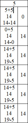
So based on the formula, the adder output must be the summation of the
value above the cell and a constant value.
For example, 5 is the constant value.
So for the first cell, 5 which is the top value and also a
initialization value is add to 5, the constant value.
As you can see in the waveform (2018-08-24_11-18_24), it is wrong
because there no the 5 value before the computation starts.
It should be a stream of input 5, 0 and 14 add with constant 5 with the
output stream of 10, 4 and 19.
So, how can I put a value and it has to be at a stream of number but on
for one clock cycle?
Hi Vancouver.
How was your holiday?
I hope you didnt forget about my question that I posted on 28 August
2018.
I really need your help.
Hope that you can reply to me as soon as possible.
Thank you.
dayana42200 wrote:> How was your holiday?
Too short, as usual :-) Sorry for the delay, sure I will try to help
you.
I tried to understand your problem but I am not sure that I got the
point. From the waveform I see that the adder works correctly - the
constant value 5 (input B) is added to each input value. Since there is
no register inside the adder, the result appears immediately at the
output.
According to the table 11-05-31, the first input value of the adder
should be 5 instead of 0 as in the waveform. The non-constant adder
input is taken from the subtractor output which is 0 in the first step.
Consider that the subtractor contains a register and has a reset input.
The register contents will be (usually) 0 after releasing the reset
input, so the subtractor output is 0 at the the beginning. So it is
clear that also the adder input is 0 in the first clock cycle after
reset. Maybe this is the problem?
For clarification you should make a waveform showing the outputs of
adder, comparator and subtractor of the second PE as well as the PE
inputs including clk and reset.
Vancouver wrote:> I tried to understand your problem but I am not sure that I got the> point. From the waveform I see that the adder works correctly - the> constant value 5 (input B) is added to each input value. Since there is> no register inside the adder, the result appears immediately at the> output.
Correct
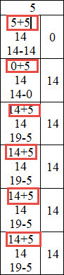
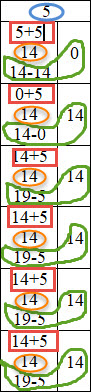
> According to the table 11-05-31, the first input value of the adder> should be 5 instead of 0 as in the waveform.
Based on the table 11-05-31,the addition output is from the A input plus
constant input B, 5 show in the red box. The value 5, in blue box at the
top of the table is the initialization value. This value 5 will be used
as is fixed initialization value for PE1 to PEn except for PE0 which the
initialization value is 0.
Please refer to schematic diagram 10-58-01. The orange circle IN TABLE
11-05-31 is the output of the comparator (Sync_Rst_CompDelTop). It is
the comparison between the additionOUT from Sync_Rst_TWO_Input_Adder and
InterA, which the output is from the other block of the same PE1. The
one in green is for the difference (Sync_Rst_TWO_Input_Sub_Top) between
the output of SCORE_DelTop and PreDelH from previous PE0. So the output
of this block (SCORE_DelTop) should be, the initialization value 5, 0
and 14.
> For clarification you should make a waveform showing the outputs of> adder, comparator and subtractor of the second PE as well as the PE> inputs including clk and reset
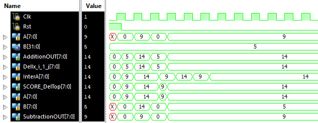
Referring to 9-39-50, the output of the adder, comparator and subtrator
is wrong and not the same as table 11-05-31. Theoretically, the addition
starts by adding the initialization value 5 and a constant, 5.
So, my question is, how can I introduce the initialization value 5 to
the adder for only one clock cycle?
Ok, as I supposed, the problem is that the register inside the
subtractor is initialized with 0 after reset. So the adder computes 0+5
instead 5+5. Due to the loop back, all consecutive results are wrong.
The solution to this problem depends on the source of initialization
value. I think that it is 5 only in this example, but in general, the
value may be different?

- If the init value will not change during runtime, you could pass it to
the subtractor as a verilog parameter and then modify the code such that
the parameter value is used as a reset value, instead 0. This is a
simple straight forward way, but a bit ugly. The reset signal should be
used only to put the system in a defined state but not for loading
parameters. However, for a quick fix, you could try this.

- A more elegant but complex way would be to implement a controller.
Currently, your design starts operating immediately after reset. It
would be better to have an init and a start signal. First, the init
signal is set for one clock cycle, and during this, the initialization
value is loaded into the subtractor register. Then the start signal is
set and the design starts with the previously loaded parameters. This is
the preferred way as it allows you to restart the computation without
reset and also to load the init value from a register. init  and start
are generated from a small state  machine.
Hi Vancouver.

I tried the initialize the rst value to 5 and it works. Thank you very
much.

I have some other problem and I need your help.

Below is my 3 input comparator used for all PEs in the design. Before I
didnt use clock here, but the output waveform some value that I didnt
want due to different in timing within the three input. So, I have to
use the clock without Rst.
3'b000: SCORE_Inter <= LUT; //All equal so doesn't matter
24
3'b001: SCORE_Inter <= DelIy_i_j_1; //C
25
3'b010: SCORE_Inter <= DelIx_i_1_j; //B
26
3'b011: SCORE_Inter <= DelIx_i_1_j; //B
27
3'b100: SCORE_Inter <= LUT; //A
28
3'b101: SCORE_Inter <= DelIy_i_j_1; //C
29
3'b110: SCORE_Inter <= LUT; //A
30
3'b111: SCORE_Inter <= 0; //- (output 0)
31
default: SCORE_Inter <= 0; //- (output 0)
32
endcase
33
end
34
endmodule
Based on the attached waveform,the 1st 4 waveform are from PE0 and the
last 4 is from PE1. The PE0 output 0 value since I didnt make any
initialization. However, for PE1 have the 0 value even though I didnt
make initialization. Do you know why? Also I have warning for this
matter during synthesize but only for PE1.

>Xst:1710 - FF/Latch <pe0/A/CompInterA/SCORE_Inter_7> (without init value) has a
constant value of 0 in block <SystolicArrayNovelty2_Testing>. This FF/Latch will
be trimmed during the optimization process.
>Xst:1895 - Due to other FF/Latch trimming, FF/Latch
<pe1/A/CompInterA/SCORE_Inter_7> (without init value) has a constant value of 0 in
block <SystolicArrayNovelty2_Testing>. This FF/Latch will be trimmed during the
optimization process.
>Xst:1895 - Due to other FF/Latch trimming, FF/Latch
<pe2/A/CompInterA/SCORE_Inter_7> (without init value) has a constant value of 0 in
block <SystolicArrayNovelty2_Testing>. This FF/Latch will be trimmed during the
optimization process.
>Xst:1895 - Due to other FF/Latch trimming, FF/Latch
<pe3/A/CompInterA/SCORE_Inter_7> (without init value) has a constant value of 0 in
block <SystolicArrayNovelty2_Testing>. This FF/Latch will be trimmed during the
optimization process.
>Xst:1895 - Due to other FF/Latch trimming, FF/Latch
<pe4/A/CompInterA/SCORE_Inter_7> (without init value) has a constant value of 0 in
block <SystolicArrayNovelty2_Testing>. This FF/Latch will be trimmed during the
optimization process.
>Xst:1895 - Due to other FF/Latch trimming, FF/Latch
<pe5/A/CompInterA/SCORE_Inter_7> (without init value) has a constant value of 0 in
block <SystolicArrayNovelty2_Testing>. This FF/Latch will be trimmed during the
optimization process.

I cant ignore this warning since it effect other output in the other
submodule.

Thank you very much
According to the warning, bit 7 of SCORE_Inter will be removed since it
is always 0. Does this warning also occur for other bits? You should
combine {dA_GreaterThan_dB,dB_GreaterThan_dC,dC_GreaterThan_dA} in a
vector and display this in the waveform to see under which circumstances
the respective case conditions occur. This may help to find out the
reason for the 0 output in PE 1. Try to use stimuli that drive bit 7 of
DelIy_i_j_1, LUT etc high. Is it possible that computations simply do
not use the full 8 bit range? Maybe the results are always positive so
bit 7 will never be set in the signed format?
Vancouver wrote:> According to the warning, bit 7 of SCORE_Inter will be removed since it is
always 0. Does this warning also occur for other bits?
>>Xst:1710 - FF/Latch <pe0/A/CompInterA/SCORE_Inter_7> (without init value) has a
constant value of 0 in block <SystolicArrayNovelty2_Testing>. This FF/Latch will
be trimmed during the optimization process.
>>Xst:1895 - Due to other FF/Latch trimming, FF/Latch <pe1/A/CompInterA
/SCORE_Inter_7> (without init value) has a constant value of 0 in block
<SystolicArrayNovelty2_Testing>. This FF/Latch will be trimmed during the
optimization process.
>>Xst:1895 - Due to other FF/Latch trimming, FF/Latch
<pe2/A/CompInterA/SCORE_Inter_7> (without init value) has a constant value of 0 in
block <SystolicArrayNovelty2_Testing>. This FF/Latch will be trimmed during the
optimization process.
>>Xst:1895 - Due to other FF/Latch trimming, FF/Latch
<pe3/A/CompInterA/SCORE_Inter_7> (without init value) has a constant value of 0 in
block <SystolicArrayNovelty2_Testing>. This FF/Latch will be trimmed during the
optimization process.
>>Xst:1895 - Due to other FF/Latch trimming, FF/Latch
<pe4/A/CompInterA/SCORE_Inter_7> (without init value) has a constant value of 0 in
block <SystolicArrayNovelty2_Testing>. This FF/Latch will be trimmed during the
optimization process.
>>Xst:1895 - Due to other FF/Latch trimming, FF/Latch
<pe5/A/CompInterA/SCORE_Inter_7> (without init value) has a constant value of 0 in
block <SystolicArrayNovelty2_Testing>. This FF/Latch will betrimmed during the
optimization process.
> You should combine {dA_GreaterThan_dB,dB_GreaterThan_dC,dC_GreaterThan_dA} in a
vector and display this in the waveform to see under which circumstances the
respective case conditions occur. This may help to find out the reason for the 0
output in PE 1.
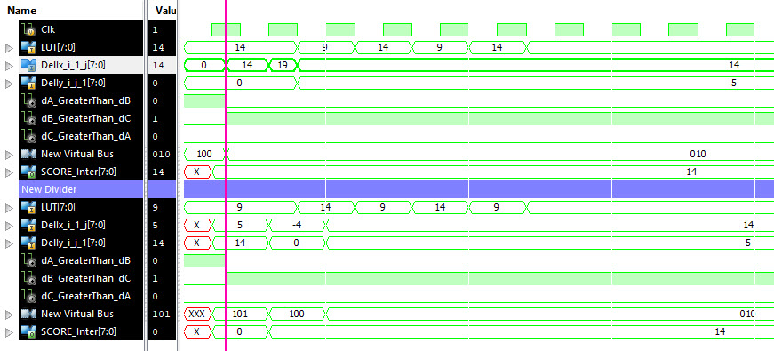
>> Ive tried your suggestion. As you can see, the waveform is divided to two
parts. The top part is for PE0 and bottom part is for PE1. Ive combine
{dA_GreaterThan_dB,dB_GreaterThan_dC,dC_GreaterThan_dA} into a bus (New Virtual
Bus) and the combination doesnt lead to o/p 0. So I think the 0 does come from the
warning.
Any idea why?


