
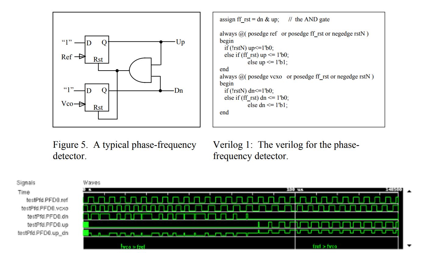
Hello , i am trying to run in Xilinx the following code of phase
detector
as shown in the attached link and attached photo.

i am not sure why up,dn should be reg?
why ff_rst is a wire why its not a reg?
what is the role of vcxo,rstN?


http://www.dtic.mil/get-tr-doc/pdf?AD=ADA483891


module phase_detector(ref,vco,up,dn);
input ref;
input vco;
output up;
output dn;

wire ref;
wire vco;
reg up;
reg dn;


assign ff_rst = dn & up; // the AND gate
always @( posedge ref or posedge ff_rst or negedge rstN )
begin
 if (!rstN) up<=1'b0;
 else if (ff_rst) up <= 1'b0;
 else up <= 1'b1;
end
always @( posedge vcxo or posedge ff_rst or negedge rstN )
begin
 if (!rstN) dn<=1'b0;
 else if (ff_rst) dn <= 1'b0;
 else dn <= 1'b1;
end

endmodule
Attached files:
-

phase_detector.JPG
140 KB
Rock B. wrote:
> what is the role of vcxo,rstN?
rstN ist a low active reset. I think this is only necessary for
simulation or asic design.

For vcxo show here:
https://en.wikipedia.org/wiki/Phase-locked_loop#Block_diagram

Duke
i cant see vcox in the diargram on the article, i am trying to implement
the code in Xilinx but its not working

module phase_detector(ref,vco,up,dn);
input ref;
input vco;
output up;
output dn;

wire ref;
wire vco;
reg up;
reg dn;


assign ff_rst = dn & up; // the AND gate
always @( posedge ref or posedge ff_rst or negedge rstN )
begin
 if (!rstN) up<=1'b0;
 else if (ff_rst) up <= 1'b0;
 else up <= 1'b1;
end
always @( posedge vcxo or posedge ff_rst or negedge rstN )
begin
 if (!rstN) dn<=1'b0;
 else if (ff_rst) dn <= 1'b0;
 else dn <= 1'b1;
end

endmodule
Rock B. wrote:
> i am trying to implement
> the code in Xilinx but its not working
That is not a valid error description.

What did you try?
Will you just simulate the code?
Where is your testbench?

Duke
Rock B. wrote:
> i cant see vcox in the diargram on the article
Its absolute obviously a typo like vcxo = vco...

> i am trying to implement the code in Xilinx
Then forget about that rstN. You don't need it.

> but its not working
How did you find that out? What do you expect? And what do you get
instead? Does your simulation look fine?

I would try it that way:
1 | module phase_detector(ref,vco,up,dn); |
2 | input ref; |
3 | input vco; |
4 | output up; |
5 | output dn; |
6 | |
7 | wire ref; |
8 | wire vco; |
9 | reg up = 1'b0; |
10 | reg dn = 1'b0; |
11 | |
12 | assign ff_rst = dn & up; // the AND gate |
13 | |
14 | always @(posedge ref or posedge ff_rst) |
15 | begin
|
16 | if (ff_rst) up <= 1'b0; |
17 | else up <= 1'b1; |
18 | end
|
19 | always @(posedge vcxo or posedge ff_rst) |
20 | begin
|
21 | if (ff_rst) dn <= 1'b0; |
22 | else dn <= 1'b1; |
23 | end
|
24 | |
25 | endmodule
|
Attached files:
-

phase_detector.JPG
140 KB
Hello,i thought to simulate it without a test bench ,in XILINX we can
force a signal and clock in the inputs.

ok , so for the variables ,why up,dn are reg type?
why ff_rst is a wire?
i cant see it the from the attached diagram


Thanks
why up,dn are reg type? why ff_rst is a wire?

Lookup the description of D-Flip-Flops. What type of signal is denoted
by "Q", what type of signal is denoted by rst ? That should answer your
question.(Remember a "Flip-Flop" closely resembles a "register")
from the manual i know that the inputs and outputs should be wires
that they are not storing data.

in this case i cant see what variable stores data and what variable does
not store data ?

Thanks
Rock B. wrote:
> in this case i cant see what variable stores data and what variable does
> not store data ?
Only the two flipflops can store values.
Hello , i tried  to implement the reg everywhere i think it stores
memory ,
i did defined dn
why ff_rst cannot be input?

Thanks

 Line 22: Port dn is not defined
 Line 23: Non-net port ff_rst cannot be of mode input
 Line 21: Module <phase_d> ignored due to previous errors.
1 | module phase_d(ref,vco,ff_rst); |
2 | output up,dn; |
3 | input ref,vco,ff_rst; |
4 | |
5 | reg dn,ff_rst; |
6 | reg up; |
7 | reg ref; |
8 | reg vco; |
9 | always @(posedge ref or posedge ff_rst) |
10 | begin
|
11 | assign ff_rst=dn&up; |
12 | if (!ff_rst) up<=1'b0; |
13 | else up<=1'b1; |
14 | end
|
15 | |
16 | always @(posedge vco or posedge ff_rst) |
17 | begin
|
18 | assign ff_rst=dn&up; |
19 | if (!ff_rst) dn<=1'b0; |
20 | else dn<=1'b1; |
21 | end
|
22 | |
23 | endmodule
|
Rock B. wrote:
> i did defined dn

but you don't have it in the port list.

> why ff_rst cannot be input?

because it's also the output of the AND gate. Just make it a wire, no
in- or output.

Look at the code in the picture of your first post to place the assign
at the right place and only once.

Andy
the code doesnt give me any errors but i am curios regarding few issues.
why assigh have to be outside always?
why the input cannot be a reg?
why ff_rst has to be a wire for being an output of AND
dn and up are output too?


Thanks
[verilog]
module phase_d(ref,vco,dn,up);
output up,dn;
input ref,vco;

wire ff_rst;
reg up,dn;


assign ff_rst=dn&up;
always @(posedge ref or posedge ff_rst)
begin

if (!ff_rst) up<=1'b0;
else up<=1'b1;
end

always @(posedge vco or posedge ff_rst)
begin
if (!ff_rst) dn<=1'b0;
else dn<=1'b1;
end

endmodule
[/verilog]
Rock B. wrote:
> why assigh have to be outside always?

assign connects wires to inputs and outputs or defines combinatorial
logic. Such signals are always active in opposite to registers which
change their state only on an active clock edge and hold the state until
the next edge.

> why the input cannot be a reg?

An input is just a wire with a defined direction, if you want to
register the state of the input you need an additional register with a
clock.

> why ff_rst has to be a wire for being an output of AND
> dn and up are output too?

ff_rts is an internal signal that connects something. The terms input
and output are only used at the ports of a module to define the
direction of the port. An output port can also directly be defined as a
register:

output reg up,dn;

or as in your code, first as an output and then as a register.
Attached files:
-

Untitled.jpg
150 KB -

Capture.JPG
85 KB
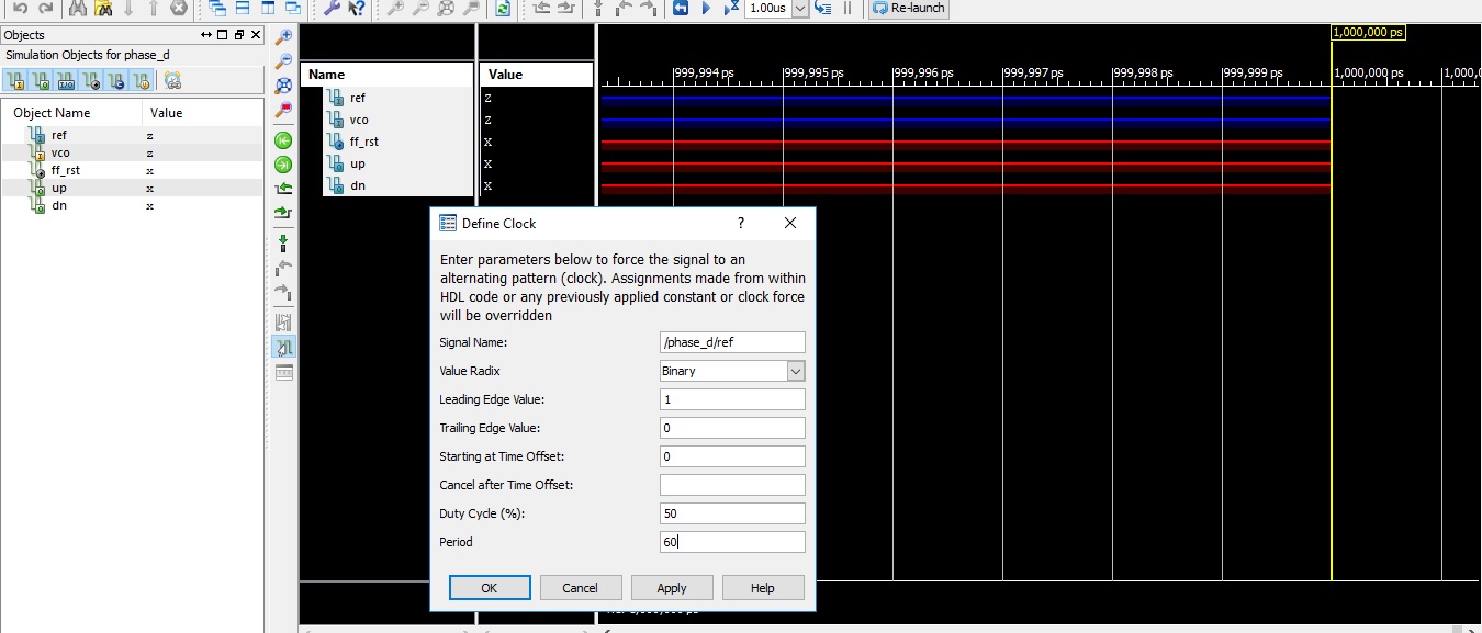
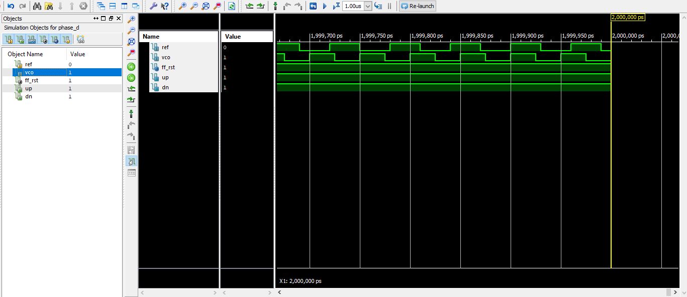
Hello in order to see the effect of the phase detection i have defined
ref and vco as shown in the attached photo.
ref as 60ps period and 50 duty cycle
vco as 50ps period and 50 duty cycle

as it shows in the attached simulation photo there is a phase shift
between the ref and vco but the up and dn aren't changing.what went
wrong?

Thanks
1 | module phase_d(ref,vco,dn,up); |
2 | output up,dn; |
3 | input ref,vco; |
4 | |
5 | wire ff_rst; |
6 | reg up,dn; |
7 | |
8 | |
9 | assign ff_rst=dn&up; |
10 | always @(posedge ref or posedge ff_rst) |
11 | begin
|
12 | |
13 | if (!ff_rst) up<=1'b0; |
14 | else up<=1'b1; |
15 | end
|
16 | |
17 | always @(posedge vco or posedge ff_rst) |
18 | begin
|
19 | if (!ff_rst) dn<=1'b0; |
20 | else dn<=1'b1; |
21 | end
|
22 | |
23 | endmodule
|
Rock B. wrote:
> if (!ff_rst) up<=1'b0;
The simulation does exactly what you have written down. If you want
something else then look at my code or use that grey thing between your
ears and answer the question:
Why the heck a NOT before ff_rst?
Attached files:
-

Capture.JPG
85 KB
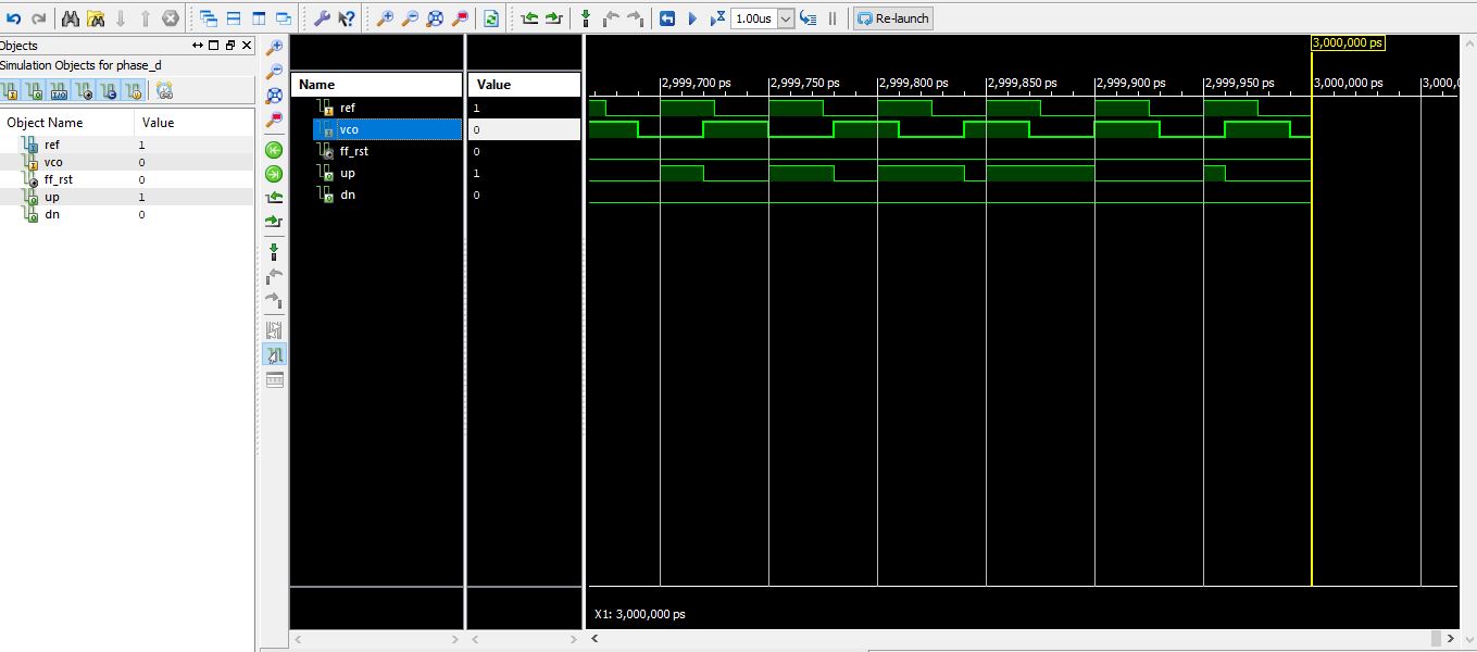
Hello , i think there is another problem  because as you can see in the
attached photo the ff_rst is zero all the way although the ref and vco
do change.it seems as if the ASIGN command ran only once,why is that?

Thanks
1 | module phase_d(ref,vco,dn,up); |
2 | output up,dn; |
3 | input ref,vco; |
4 | |
5 | wire ff_rst; |
6 | reg up=1'b0; |
7 | reg dn=1'b0; |
8 | |
9 | |
10 | assign ff_rst=dn&up; |
11 | always @(posedge ref or posedge ff_rst) |
12 | begin
|
13 | |
14 | if (ff_rst) up<=1'b0; |
15 | else up<=1'b1; |
16 | end
|
17 | |
18 | always @(posedge vco or posedge ff_rst) |
19 | begin
|
20 | if (ff_rst) dn<=1'b0; |
21 | else dn<=1'b1; |
22 | end
|
23 | |
24 | endmodule
|
Rock B. wrote:
> the ff_rst is zero all the way
I don't think so, because the up-flipflop is reset at each rising edge
of vco. The thing is: the ff_rst is high only for one timestep within
the same simulation cycle.

Or with other words: as far as i can see the simulation does exactly
what it should. The up flipflop goes high at the rising edge of ref, and
it is reset when vco rises also.
The only problem is here, that the frequency of one input is always
higher than the other. Change the both input frequencies and look whats
happening.
Hello, why the 'dn' is always zero?
There are places where VCO rises and because ff_rest is always zero then
dn should go to '1' every time VCO rise
it meet the criteria of the always@ part bellow.
Thanks
1 | always @(posedge vco or posedge ff_rst) |
2 | begin
|
3 | if (ff_rst) dn<=1'b0; |
4 | else dn<=1'b1; |
5 | end
|
Rock B. wrote:
> Hello, why the 'dn' is always zero?
Did you swap the two input signals? What happened?

> There are places where VCO rises and because ff_rest is always zero then
> dn should go to '1'
Can't see such occurrences.
And when the two input signals are constant and stable, then why
should the output change?
Attached files:
-

Capture.JPG
36 KB
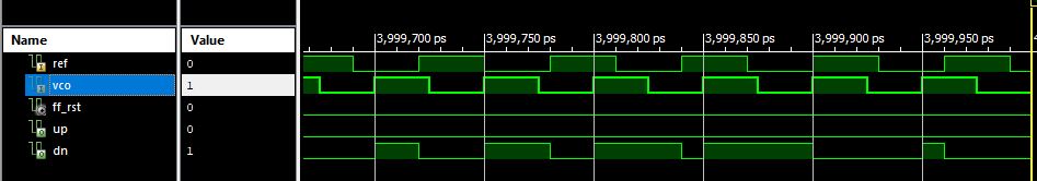
Hello ,Yes when i switched the signals up=0 all the way as you can see
in the attached photo.

so for the first always@ ff_rst=0 all the time thus making up=0 the
whole time as we can see in the result.

but for the second always@  ff_rst is not always zero because dn do get
to be 1 some times

because we have only one ff_rst  then we should have or both 'dn' and
'up' zero or both of them toggeling by the VCO and ref clocks?
1 | always @(posedge ref or posedge ff_rst) |
2 | begin
|
3 | |
4 | if (ff_rst) up<=1'b0; |
5 | else up<=1'b1; |
6 | end
|
1 | always @(posedge vco or posedge ff_rst) |
2 | begin
|
3 | if (ff_rst) dn<=1'b0; |
4 | else dn<=1'b1; |
5 | end
|
Ok, let's resume: the code is working as expected. And let me propose,
that the synthesized hardware will look as the hardware in the picture.
So the only problem is, that you can't recognize and accept that.

With other words: of course ff_rst goes high! But you can't see it
directly, because at the very same moment both flipflops go low and so
at the very same time ff_rst goes low again. This happens in 0 (in
words: zero) ps, because you are doing a behavioural simulation which
has absolutely no (in numbers 0) delay!

Think about this: the only way to reset the flipflops is by ff_rst going
high. At the very same time when dn or up goes from 1 to 0 the signal
ff_rst must have been 1.

Think about that. It isn't that difficult...

When nothing works for you then try a post route simulation.
Please log in before posting. Registration is free and takes only a minute.
Existing account
Do you have a Google/GoogleMail account? No registration required!
Log in with Google account
Log in with Google account
No account? Register here.