EmbDev.net

Forum: FPGA, VHDL & Verilog LUT utilization is 121 %


von Lakshita J. (lakshita)


Rate this post
useful
not useful
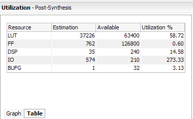
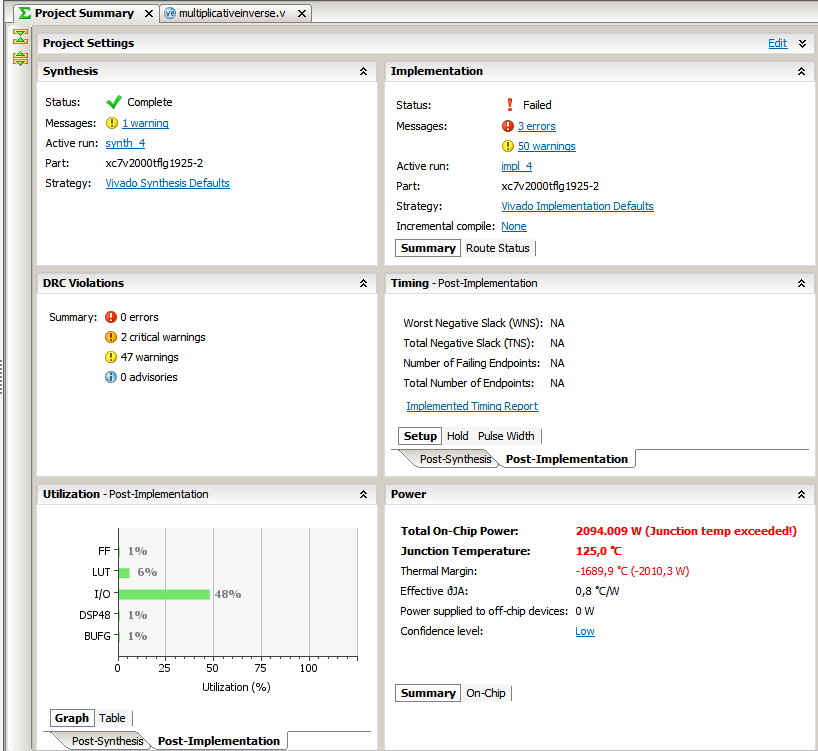
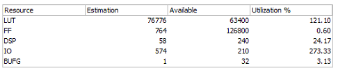
Hi
I am working on a multiplicative inverse algorithm to implement ecc 
algorithm. I have made the Verilog code for this, The simulation is 
working properly but the synthesis report is showing LUT utilization 
76776 out of 63400.I have applied DSP attribute to reduce no of LUTs and 
it reduces from 78000 to 76776
I am targeting Nexys4DDR FPGA board
Please provide any solution to minimize LUT utilization.I have attached 
project summary and utilization report of this code.
1
(* use_dsp48 = "yes" *)
2
module multiplicative_inverse #(parameter n = 190)(clk, reset, enable, p, a, x, result_ready);
3
  input clk, reset, enable;
4
  input wire [n-1:0] p;
5
  input wire [n-1:0] a ;
6
   output reg [n-1:0] x;
7
  output reg result_ready;
8
9
  //flag to initialize variables when reset
10
 reg flag;
11
  
12
   reg [n-1:0] Y;
13
   reg [n-1:0] D; 
14
   reg [n-1:0] B;
15
 
16
   wire Y0 = (Y[0] == 0) ? 1 : 0;
17
   wire D0 = (D[0] == 0) ? 1 : 0;
18
19
  reg flagY0 = 1;
20
  reg flagD0 = 1;
21
 
22
 
23
24
  
25
26
  always @ (posedge clk) begin
27
    if (reset) begin
28
      x <= 0;
29
      flag <= 1;
30
      result_ready <= 0;
31
    end
32
    else  begin
33
      if(result_ready) begin
34
        result_ready <= 0;
35
        flag <= 1;
36
      end
37
      else //Initialize the variables
38
      if (flag || enable) begin
39
        Y <= a;
40
        D <= p;
41
        B <= 1;
42
        x <= 0;
43
        flag <= 0;
44
      end
45
      else begin
46
    
47
        if (Y != 0) begin
48
        
49
          if (Y0 && flagY0) begin
50
           
51
            Y = Y >> 1;
52
           
53
      
54
            B = (B + (B[0]*p)) >> 1;
55
     
56
          end //end if
57
        
58
          else begin
59
            flagY0 = 0;
60
          end
61
          if (D0 && flagD0) begin
62
      
63
            D = D >> 1;
64
            x = (x + (x[0]*p)) >> 1;
65
         
66
          end //end if
67
          else begin
68
            flagD0 = 0;
69
          end
70
         if((flagY0 == 0) && (flagD0 == 0)) begin
71
         
72
            if (Y >= D) begin
73
              Y = Y - D;
74
              if(B < x) 
75
            
76
              B = B + p ;
77
              B = (B - x) % p;
78
              
79
            end
80
            else begin
81
              if(D < Y) 
82
              D = D + p;
83
              D = D - Y;
84
              if(x < B)
85
              x = x + p;
86
              x = (x - B) % p;
87
            end //else
88
            flagY0 = 1;
89
            flagD0 = 1;
90
          end //else
91
        end //end if
92
        else begin
93
          result_ready <= 1;
94
        end
95
      end
96
    end
97
  end
98
endmodule

: Edited by Moderator
von Guest (Guest)


Rate this post
useful
not useful
I'm guessing you're trying to find
 such that
 with
.

I'm not quite sure as to how your algorithm is supposed to work since 
you're neither properly naming your signals nor giving any comments as 
to their functionality. However you're instantiating at least 2 190 bit 
modulo operators which should be a dead giveaway as to where the 
resources are going. You're also going to see some ridiculous timing 
violations on these paths.

Each of these is going to have in the order of
 LUTs since it's basically doing a test-subtraction of a shifted value 
of p for every bit.

At least the solution is simple, get a bigger FPGA or write a better 
algorithm. Your choice.

von Guest (Guest)


Rate this post
useful
not useful
Oh i forgot to mention, if it were just one LUT per bit that would turn 
out to be almost 18k LUTs per '%' in your code, i.e. 36k. Probably it's 
more like 2 LUTs per bit or something...

von Lothar M. (Company: Titel) (lkmiller) (Moderator)


Rate this post
useful
not useful
Lakshita J. wrote:
> x = (x - B) % p;
Try that combinatorial division (a modulo value is only the remainder of 
a division) with a very simple "three-line-design": just divide 2 input 
vectors and assign the result to an output vector. Start with two 8 bit 
vectors, increase the length to 16, 32, 64, 128 and at last 190 bits and 
look für the resource consumption and the speed/delay of the design.

This here gives 33k LUTs in a Spartan3 for a 160/80 bits design:
Beitrag "Re: Rechnen mit unsigned vs. signed und einer division"
And its rather slow: max. clock frequency is 1 MHz...   :-o

von Lakshita J. (lakshita)


Attached files:

Rate this post
useful
not useful
Thanks for the valuable information.
operator % was taking lot of resources.I somehow manage to get down the 
no of LUTS and now the consumption is 37226 out of 63400.
But there is problem regarding input output pin,the availability is 210 
and
I am getting 574 because the input & output are of 192 bits.Due to this 
implementation is getting failed.
Please provide any solution for this too.

von Duke Scarring (Guest)


Rate this post
useful
not useful
You need a chip with more I/O-pins. Or you find a solution to get your 
data in and out in a serial or partial serial way.

Duke

von Lakshita J. (lakshita)


Attached files:

Rate this post
useful
not useful
Hello,

I have used virtual input output concept to get down number of pins.The 
synthesis ,implementation and bit stream generation is working 
properly.but when I programmed it to FPGA,the output showing 0 results 
and during implementation the summary report is showing router estimated 
timing not net.
I have attached the timing report and output results.
If anybody knows how to use  virtual input output(VIO),then please 
provide any solution to above problem.

von Duke Scarring (Guest)


Rate this post
useful
not useful
Lakshita J. wrote:
> but when I programmed it to FPGA,the output showing 0 results
Do you have a testbench, which shows the expected results?

Duke

von Lakshita J. (lakshita)


Attached files:

Rate this post
useful
not useful
I have attached testbench file and simulation results.

von Duke Scarring (Guest)


Attached files:

Rate this post
useful
not useful
Lakshita J. wrote:
> I have used virtual input output concept to get down number of pins.The
> synthesis ,implementation and bit stream generation is working
> properly.but when I programmed it to FPGA,the output showing 0 results
> and during implementation the summary report is showing router estimated
> timing not net.
> I have attached the timing report and output results.
> If anybody knows how to use  virtual input output(VIO),then please
> provide any solution to above problem.

The given code simulates (after some small changes). Synthesis work only 
with the xc7v2000tflg1925 device.

For debugging I suggest to use a clear smaller number than 190 for n.
Start with n = 8 or n = 16. Than you can more easely what's going wrong 
with n = 190.

Duke

von Lakshita J. (lakshita)


Attached files:

Rate this post
useful
not useful
> For debugging I suggest to use a clear smaller number than 190 for n.
> Start with n = 8 or n = 16. Than you can more easely what's going wrong
> with n = 190.

I tried for n=5,20,60,80,100 bits,I am getting some value but when I 
move above 100 bits the Hardware server gets shut down and it 
automatically gets disconnect.I have attached the screen shot for this 
problem and also I have attached screen shot for 100 bit results.
Please provide any solution for this problem.

von Duke Scarring (Guest)


Rate this post
useful
not useful
So you find a limitation in Hardware server.
I never used Hardware server, so I can't say anything about it.

You need to find another way to communicate with you multiplier.
What hardware interfaces exists on your board? UART? Ethernet?

Duke

Please log in before posting. Registration is free and takes only a minute.
Existing account
Do you have a Google/GoogleMail account? No registration required!
Log in with Google account
No account? Register here.