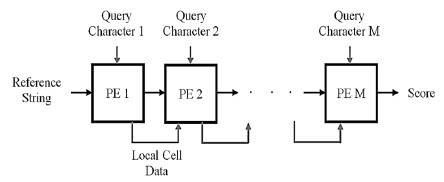
Hi everyone. Currently Im designing systolic array using Verilog HDL.
Systolic array is consist of an array of Processing Element (PE). The
design is synthesise usng Xilinx ISE.

Below is my previous design for 2 PEs.
if (i == 0) //first processing element in auto-generated chain
29
begin:pe
30
ProcessingElement pe0
31
( .Clk (Clk),
32
.Rst (Rst),
33
.SS (SubSec[2:0]),
34
.QC (QueSec[2:0]),
35
.Gap (Gap[2:0]),
36
.DDiag (15'b0),
37
.DTop (15'b0),
38
.DLeft (15'b0),
39
.LDiag (15'b0),
40
.LLeft (15'b0),
41
.Zero (15'b0),
42
.SCORE_PE_Previous (15'b0),
43
.DiagOut (d[i]),
44
.LeftOut (l[i]),
45
.TopOut (t[i]),
46
.SCORE_Left_D (dl[i]),
47
.SS_Out (SSout[2:0]),
48
.Gap_Out (GAPout[2:0]),
49
.Best_So_Far_PE_SCORE (score[i])
50
);
51
end
52
else //processing elements other than first one
53
begin:pe
54
ProcessingElement pe1
55
( .Clk (Clk),
56
.Rst (Rst),
57
.SS (SSout[(3*i)-1:(3*i)-3]),
58
.QC (QueSec[(3*i)+2:3*i]),
59
.Gap (GAPout[(3*i)-1:(3*i)-3]),
60
.DDiag (d[i-1]),
61
.DTop (t[i-1]),
62
.DLeft (dl[i-1]),
63
.LDiag (d[i-1]),
64
.LLeft (l[i-1]),
65
.Zero (15'b0),
66
.SCORE_PE_Previous (score[i-1]),
67
.DiagOut (d[i]),
68
.LeftOut (l[i]),
69
.TopOut (t[i]),
70
.SCORE_Left_D (dl[i]),
71
.SS_Out (SSout[(3*i)+2:3*i]),
72
.Gap_Out (GAPout[(3*i)+2:3*i]),
73
.Best_So_Far_PE_SCORE (score[i])
74
);
75
end
76
end
77
endgenerate
78
endmodule
The problem with this design is that the Query input is large (3*no of
PE).
If i want to generate 100 PEs, it is impossible as it can only fit up to
75 PEs for the available I/O of the choosen devices (shown in the
attached image).

So if come with another solution shown below.
1
moduleSA_Test1(Clk,Rst,SubSec,Gap,Score);
2
3
parameterComputeDataWidth=8;
4
parameterPE=8;//LENGTH
5
6
localparam
7
N_A=3'b000,//nucleotide "A"
8
N_C=3'b001,//nucleotide "C"
9
N_G=3'b010,//nucleotide "G"
10
N_T=3'b011,//nucleotide "T"
11
G_P=3'b100;//gap '-'
12
13
inputClk,Rst;
14
input[2:0]SubSec,Gap;
15
outputsigned[ComputeDataWidth-1:0]Score;
16
17
18
wire[ComputeDataWidth-1:0]d[PE-1:0];
19
wire[ComputeDataWidth-1:0]t[PE-1:0];
20
wire[ComputeDataWidth-1:0]l[PE-1:0];
21
wire[ComputeDataWidth-1:0]score[PE-1:0];
22
wire[PE*3-1:0]SSout,GAPout;
23
24
assignScore=score[PE-1];
25
26
genvari;
27
28
generate
29
for(i=0;i<PE;i=i+1)
30
begin:pe_block
31
if(i==0)//first processing element in auto-generated chain
32
begin:pe
33
ProcessingElementpe0
34
(.Clk(Clk),
35
.Rst(Rst),
36
.SS(SubSec),
37
.QC({N_T}),
38
.Gap(Gap),
39
.DDiag(8'b0),
40
.DTop(8'b0),
41
.DLeft(8'b0),
42
.LDiag(8'b0),
43
.LLeft(8'b0),
44
.Zero(8'b0),
45
.SCORE_PE_Previous(8'b0),
46
.DiagOut(d[i]),
47
.LeftOut(l[i]),
48
.TopOut(t[i]),
49
.SS_Out(SSout[2:0]),
50
.Gap_Out(GAPout[2:0]),
51
.Max_PE_Score(score[0])
52
);
53
end
54
if(i==1)
55
begin:pe
56
ProcessingElementpe1
57
(.Clk(Clk),
58
.Rst(Rst),
59
.SS(SSout[(3*i)-1:(3*i)-3]),
60
.QC({N_G}),
61
.Gap(GAPout[(3*i)-1:(3*i)-3]),
62
.DDiag(d[i-1]),
63
.DTop(t[i-1]),
64
.DLeft(l[i-1]),
65
.LDiag(d[i-1]),
66
.LLeft(l[i-1]),
67
.Zero(8'b0),
68
.SCORE_PE_Previous(score[i-1]),
69
.DiagOut(d[i]),
70
.LeftOut(l[i]),
71
.TopOut(t[i]),
72
.SS_Out(SSout[(3*i)+2:3*i]),
73
.Gap_Out(GAPout[(3*i)+2:3*i]),
74
.Max_PE_Score(score[i])
75
);
76
end
77
if(i==2)
78
begin:pe
79
ProcessingElementpe2
80
(.Clk(Clk),
81
.Rst(Rst),
82
.SS(SSout[(3*i)-1:(3*i)-3]),
83
.QC({N_C}),
84
.Gap(GAPout[(3*i)-1:(3*i)-3]),
85
.DDiag(d[i-1]),
86
.DTop(t[i-1]),
87
.DLeft(l[i-1]),
88
.LDiag(d[i-1]),
89
.LLeft(l[i-1]),
90
.Zero(8'b0),
91
.SCORE_PE_Previous(score[i-1]),
92
.DiagOut(d[i]),
93
.LeftOut(l[i]),
94
.TopOut(t[i]),
95
.SS_Out(SSout[(3*i)+2:3*i]),
96
.Gap_Out(GAPout[(3*i)+2:3*i]),
97
.Max_PE_Score(score[i])
98
);
99
end
100
if(i==3)
101
begin:pe
102
ProcessingElementpe3
103
(.Clk(Clk),
104
.Rst(Rst),
105
.SS(SSout[(3*i)-1:(3*i)-3]),
106
.QC({N_T}),
107
.Gap(GAPout[(3*i)-1:(3*i)-3]),
108
.DDiag(d[i-1]),
109
.DTop(t[i-1]),
110
.DLeft(l[i-1]),
111
.LDiag(d[i-1]),
112
.LLeft(l[i-1]),
113
.Zero(8'b0),
114
.SCORE_PE_Previous(score[i-1]),
115
.DiagOut(d[i]),
116
.LeftOut(l[i]),
117
.TopOut(t[i]),
118
.SS_Out(SSout[(3*i)+2:3*i]),
119
.Gap_Out(GAPout[(3*i)+2:3*i]),
120
.Max_PE_Score(score[i])
121
);
122
end
123
if(i==4)
124
begin:pe
125
ProcessingElementpe4
126
(.Clk(Clk),
127
.Rst(Rst),
128
.SS(SSout[(3*i)-1:(3*i)-3]),
129
.QC({N_C}),
130
.Gap(GAPout[(3*i)-1:(3*i)-3]),
131
.DDiag(d[i-1]),
132
.DTop(t[i-1]),
133
.DLeft(l[i-1]),
134
.LDiag(d[i-1]),
135
.LLeft(l[i-1]),
136
.Zero(8'b0),
137
.SCORE_PE_Previous(score[i-1]),
138
.DiagOut(d[i]),
139
.LeftOut(l[i]),
140
.TopOut(t[i]),
141
.SS_Out(SSout[(3*i)+2:3*i]),
142
.Gap_Out(GAPout[(3*i)+2:3*i]),
143
.Max_PE_Score(score[i])
144
);
145
end
146
if(i==5)
147
begin:pe
148
ProcessingElementpe5
149
(.Clk(Clk),
150
.Rst(Rst),
151
.SS(SSout[(3*i)-1:(3*i)-3]),
152
.QC({N_G}),
153
.Gap(GAPout[(3*i)-1:(3*i)-3]),
154
.DDiag(d[i-1]),
155
.DTop(t[i-1]),
156
.DLeft(l[i-1]),
157
.LDiag(d[i-1]),
158
.LLeft(l[i-1]),
159
.Zero(8'b0),
160
.SCORE_PE_Previous(score[i-1]),
161
.DiagOut(d[i]),
162
.LeftOut(l[i]),
163
.TopOut(t[i]),
164
.SS_Out(SSout[(3*i)+2:3*i]),
165
.Gap_Out(GAPout[(3*i)+2:3*i]),
166
.Max_PE_Score(score[i])
167
);
168
end
169
if(i==6)
170
begin:pe
171
ProcessingElementpe6
172
(.Clk(Clk),
173
.Rst(Rst),
174
.SS(SSout[(3*i)-1:(3*i)-3]),
175
.QC({N_T}),
176
.Gap(GAPout[(3*i)-1:(3*i)-3]),
177
.DDiag(d[i-1]),
178
.DTop(t[i-1]),
179
.DLeft(l[i-1]),
180
.LDiag(d[i-1]),
181
.LLeft(l[i-1]),
182
.Zero(8'b0),
183
.SCORE_PE_Previous(score[i-1]),
184
.DiagOut(d[i]),
185
.LeftOut(l[i]),
186
.TopOut(t[i]),
187
.SS_Out(SSout[(3*i)+2:3*i]),
188
.Gap_Out(GAPout[(3*i)+2:3*i]),
189
.Max_PE_Score(score[i])
190
);
191
end
192
if(i==7)
193
begin:pe
194
ProcessingElementpe7
195
(.Clk(Clk),
196
.Rst(Rst),
197
.SS(SSout[(3*i)-1:(3*i)-3]),
198
.QC({N_A}),
199
.Gap(GAPout[(3*i)-1:(3*i)-3]),
200
.DDiag(d[i-1]),
201
.DTop(t[i-1]),
202
.DLeft(l[i-1]),
203
.LDiag(d[i-1]),
204
.LLeft(l[i-1]),
205
.Zero(8'b0),
206
.SCORE_PE_Previous(score[i-1]),
207
.DiagOut(d[i]),
208
.LeftOut(l[i]),
209
.TopOut(t[i]),
210
.SS_Out(SSout[(3*i)+2:3*i]),
211
.Gap_Out(GAPout[(3*i)+2:3*i]),
212
.Max_PE_Score(score[i])
213
);
214
end
215
end
216
endgenerate
217
endmodule
However, I found it hard to copy all this foe 100 PEs and change the DNA
character at QC input.

Can anyone give me some idea hoe to improve this design?
Dayana S. wrote:> However, I found it hard to copy all this foe 100 PEs and change the DNA> character at QC input.
If I understand you correctly, you want to assign a constant to the QC
input of each PE individually, so you have to write each PE instance
individually as shown in your second example. This is necessary since
you have defined the nucleotide codes as individual localparams.
It would be much easier to generate all PEs in a loop and connect the
ports to signals that are indexed by the loop index (as you have done
for the other signals). For doing so, you need define an array holding
all nucleotide codes that need to be assigned to the QC input and then
address this array with the loop index as well.
Of course you have to specify an array with as many entries as the
number of PEs, but this is much less work than writing each PE instance
by hand.
If this is not your problem... sorry then I do not understand what your
problem is.
Vancouver wrote:> For doing so, you need define an array holding> all nucleotide codes that need to be assigned to the QC input and then> address this array with the loop index as well.
This type of array
wire [ComputeDataWidth-1:0] d [PE-1:0];
Is that what u mean?
I mean something like that (just an outline in pseudo-Verilog, you have
to use the correct syntax)

wire [2:0] nucleotide [99:0];

initial begin
  nucleotide[0]  = 3'b011; // N_T goes into PE0
  nucleotide[1]  = 3'b010; // N_B goes into PE1
...
  nucleotide[7]  = 3'b010; // N_A goes into PE7
...
  nucleotide[99] = 3'bwhetwever; // N_x goes into PE99
end

// generate loop for the PEs:

for (i=0; <100; i++)
   ProcessingElement pe
              (  .Clk                       (Clk),
                 .Rst                       (Rst),
                 .SS                        (SSout[(3*i)-1:(3*i)-3]),
                 .QC                        (nucleotide[i]), // HERE!!!!
                 .Gap                       (GAPout[(3*i)-1:(3*i)-3]),
                     ...
               );
end


Did you get the point?
Btw, does the Query input (QueSec) in your first example change
completely in every clock cycle? If not, you could load the QueSec
vector sequentially (e.g. 32-bit word sequentially) into an internal
shift register before starting computation. This will save ressources if
your platform is IO-constrained.
Vancouver wrote:> Btw, does the Query input (QueSec) in your first example change> completely in every clock cycle?
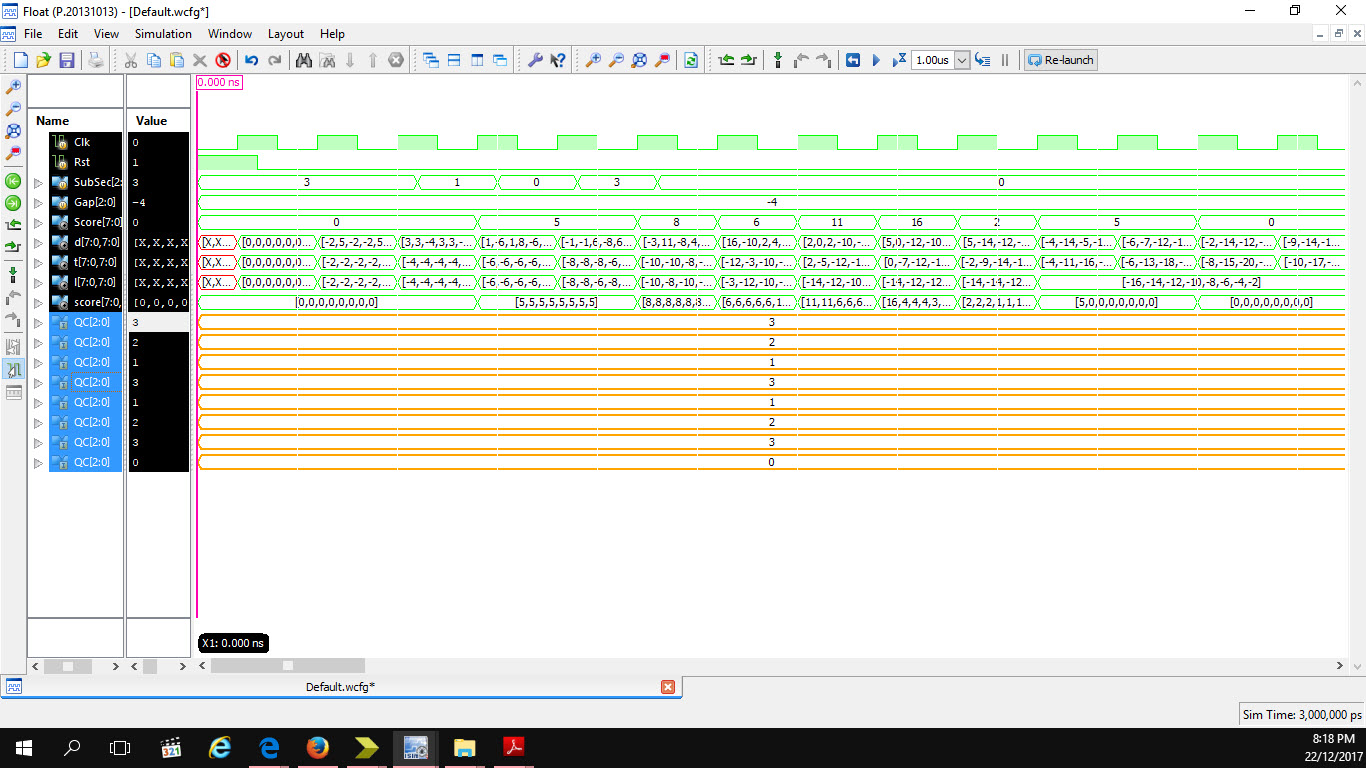
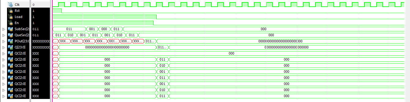
No, the input is not clocked.
The 1st waveform attached as the waveform for example 2 which is the
output that I want.
> If not, you could load the QueSec> vector sequentially (e.g. 32-bit word sequentially) into an internal> shift register before starting computation. This will save ressources if> your platform is IO-constrained.
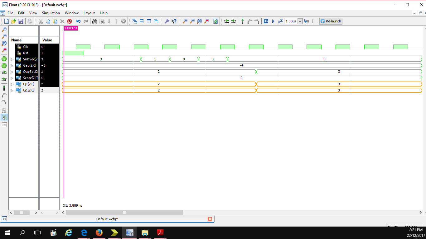
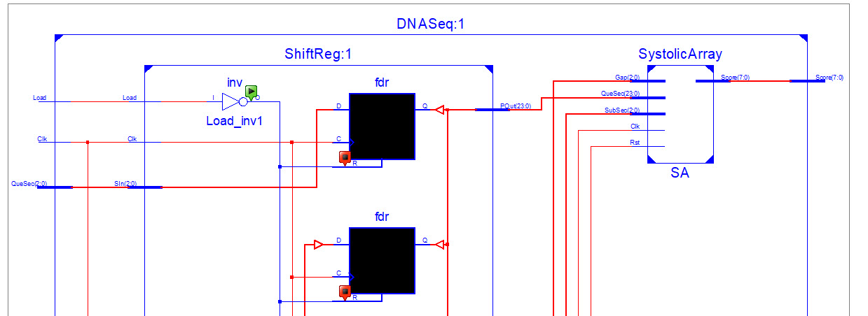
I tried the above mention method too. But the waveform is not the same
as the the first waveform attached in the second waveform. I do not
really know why. The schematic diagram shown in third attachment.
This is my shift register verilog code:
`timescale 1ns / 1ps
module ShiftReg (Clk,En,In,Out);
input Clk,En;
input [2:0] In;
output [2:0] Out;
reg [5:0] sr ; //3 x 2QC = 6 bits
always@(posedge Clk)
begin
if (En)
begin
sr <= 1;
end
else
begin
sr <= {sr[2:0],In}; //shift by 3 and concatenate Input
end
end
assign Out = sr[5:3]; //top 3 bits to output
endmodule
Hm, currently it is not clear to me what you are doing here. Let me
recapitulate. You have a number of processing elements, lets say 8, and
each PE has a 3-bit wide QC-input. Before starting the array processing,
a certain value must be applied to the QC input of each PE which remains
constant for a certain time. Is that correct? That is what I can see in
your first timing diagram.

Furthermore, you do not have enough FPGA pins to apply QC-values
directly from FPGA ports, if you have a larger number of PEs, lets say
100. So you changed your design such that the QC-Values  are hard-coded
in the FPGA design, as you did in example 2. This clearly saves FPGA
pins, but for the downside you have to make a new FPGA design each time
the constants need to be changed. Correct?

My suggestion is as follows for n PE: To keep it as simple as possible,
build a shift register of length 3*n and 1 bit wide. This register can
be loaded bit serially in a similar way as in your code in
https://embdev.net/topic/441489#5252091
The output of the shift register however, needs to be parallel. The bits
0..2 go into QC input of PE0, bits 3..5 go into PE1 and so on.
Generally, bits 3k...3k+2 go into PE[k], k=0...numberPE

Here is an example code (not tested, please check by yourself):
1
module ShiftReg (clk, reset, load, SIn, POut);
2
3
input clk, reset, load, SIn;
4
output [3*8-1:0] POut;
5
6
reg [3*8-1:0] sr ; //3 x 8QC = 24 bits
7
8
always@(posedge clk)
9
begin
10
if (reset) // reset shift register to all-zero
11
begin
12
sr <= 0;
13
end
14
else if (load=1) // enable serial load of the shift register
15
begin
16
sr <= {sr[3*8-2:0], SIn}; //shift by 1 and concatenate Input
17
end
18
end
19
20
assign POut = sr; // complete shiftreg is parallel output
Vancouver wrote:
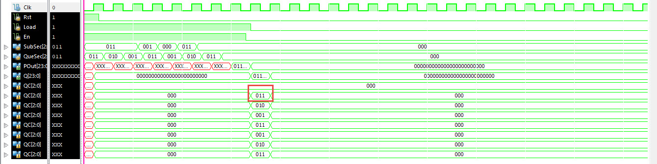
Yes ... what you mentioned is true.
Ive tried to connect SIPO and SA.
As you can see in the attachment, the nucleotide is a bit off.
I think I need a signal to choose a valid data (circled) for all the QCs
input.
What do you think?
Sorry I am only occasionally online these days.

Of course while serially loading the shiftreg, the parallel outputs show
up some garbage. If this is a problem for the PE, your either need an
additional register stage (3*n bits wide)  at the output of the SIPO and
which is clocked only once after the SIPO contents have become stable.
The other way would be just to stop the PE chain while loading the SIPO,
i.e. an enable input on each PE which keeps the PE from working (which
is the preferred method).

What do mean with a signal to choose a valid data? After loading, the
SIPO should contain only valid data at the right output for each PE.
This is the purpose of the SIPO. Only during loading, the SIPO is
inconsistent, as said above.
Vancouver wrote:> Sorry I am only occasionally online these days.
Its ok ... Its festive season. :)
> If this is a problem for the PE, your either need an additional register> stage (3*n bits wide) at the output of the SIPO and> which is clocked only once after the SIPO contents have become stable.
You mean a register with enable? or a signal that can pass the stable
SIPO content to SA?
> The other way would be just to stop the PE chain while loading the SIPO,> i.e. an enable input on each PE which keeps the PE from working (which> is the preferred method).
I dont have enable input for each PE. So i prefer the top method.
Hi, happy new year.

Ive try your opinion.

Attach is the schematic diagram and waveform.

Its working as I wanted.


However I have 1 little problem.

In the waveform, the nucleotides for all the QC's inputs are 40 ns.
Previously, the Subject Sequence (SS) was 40 ns for each Nucleotide.

Should I reduce the time for SS to fit in 40 ns?
Hi,

also my best wishes for you for the new year! I am happy to see that you
succeeded with your design. Yes I meant a register that passes the SIPO
contents to the PE chain as soon as the SIPO is fully loaded.

About the timing: A timing delay of 40ns is incredible large. Are these
diagrams from a simulation? If so, the timing specs in the source code
are irrelevant, they are ignored by the synthesis tools. The real timing
in the final FPGA design results from the placement and routing and the
number of logic levels. Timing in the FPGA can be controlled by giving
timing constraints to the synthesis tools (you must read the timing
constraints guide of you tools). In many cases, a specification of a
clock frequency is sufficient. The tools will try to make a design that
can operate at the specified clock. If this is not possible, you will
get a timing error in the tool reports. Are you using Vivado or ISE?
What clock frequency are you planning to use in your real FPGA?
I see. I didnt notice that 40 ns is too fast.
Yup that is a timing diagram from a functional simulation.
Im using ISE

Im not really sure what clock frequency I should use.
Actually, I tried any clock frequency that did not have any hold any
setup violations during timing analysis.
I have used the clock frequency reported during synthesis as benchmark
and to find the fastest clock frequency.
It is wrong?

I have another problem.
In the previous functional waveform attached, my QC is 40ns since the
output is updated every clock cycle (squared).
If I reduce the period, the QC period will also reduce.
I need QC input longer that 40ns.

Should I add more flip flops FF after the SIPO to make it longer?
Hi,

you should use the following strategy:

1. Do a pure functional simulation without any timing considerations.
Just take care that your design provides correct results. You can use
any clock frequency for simulation, since all gate delays are assumed to
be zero for now. Only count clock cycles here, but not nanoseconds.

2. Specify a performance that you like to get from your design. How many
computation results per second do you want to obtain? "As fast as
possible" is not a meaningful guide. From the functional simulation you
can see how many clock cycles per result are required, and specifying a
clock period gives you an absolute time. If you have no idea, assume
100MHz for the beginning, which is a frequency that you can reach on
most modern FPGA architectures without too much effort. A good starting
point may also to compare against a pure software implementation.

3. Decide what hardware platform you will use. What FPGA type is
planned? Is it an evaluation board or any custom-designed platform? The
performance of your design is heavily affected by the interfaces that
you will use. How do you get data into the FPGA and how the results out
of it?. Possibly all this hardware stuff is not your job and you just
want to design an IP core that will be used by somebody else. Good for
you. Proceed with 4) :-)

4. Once you have fixed a clock frequency, create an FPGA bitfile and see
whether you can reach the clock rate. There are many ways to influence
the effort of the design tools. If you cannot reach the desired clock
rate, you need to modify your design, i.e. insert additional register
stages. However: Never start with this step. You QC issue is not a
timing problem. It is a functional problem that you need so solve in (1)


About you QC problem: If I understand correctly, you need the QC input
to be unchanged for more than one lock cycle. This can be reached by a
register stage with an enable input. The enable is granted only when the
register content is allowed to change. For the enable you will need a
state machine that counts clock cycles and sets the enable every 40
clock cycles or whatever you need.
Hi :)

The QC input works. thank you for teaching me.

Also thanks for strategies that you shared.

Can I ask for your opinion for my design?
Attached is a desgin of 2 adder and 1 comparator.
As you can see I have one loop connected from the output the comparator
to a input of one of the adders. The functional simulation (attached)
doesnt show the desired function. Im aware that functional loop is bad
for a design. How can I redesign it?

Thank you.
You're welcome.

Functional loop are very common, every state machine and every counter
contains one. I think what you mean are combinatorial loops. These are
problematic, but there is no combinatorial loop in your design since all
operators are clocked.

In order to tell you what is wrong with your design, I should know the
purpose of it. Please explain what you expect from it if it would work
correctly. And please post the HDL code instead of the schematics, it is
easier to understand (at least for me).
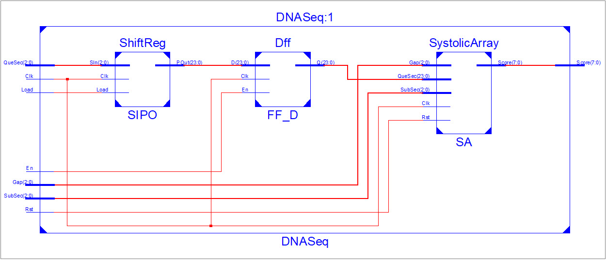
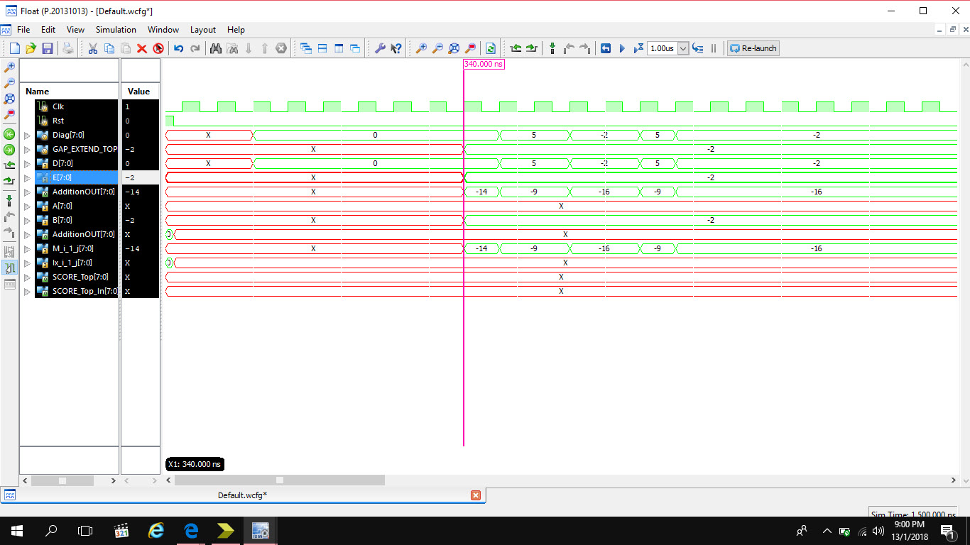
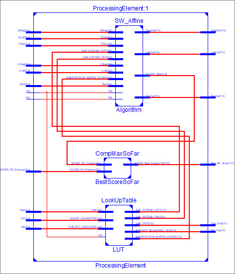
Hi :)
My Design consist of 3 modules (Figure 1), ShiftReg, Dff and SA. As Ive
mentioned, SA consist of an array of PE. Each PE has 3 modules (Figure
2), LUT, SW_Affine and MAXScore. SW_Affine is the direct implementation
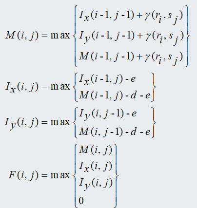
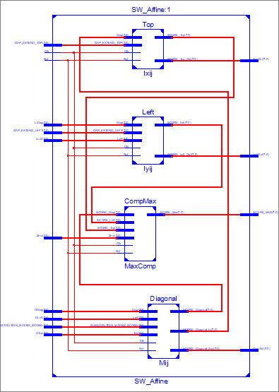
of Smith Waterman algorithm with affine gap penalty (Figure 3). So, the
submodule for SW_Affine are Diagonal, Top, Left and 4-input comparator
(Figure 4).
So for now im having a computation problem at Top sub module (Figure 5).
The computation start there is a comparision of stabilized QC and SubSec
at 340ns (Figure 6) . Thus Ive delayed SubSec until the data is compared
with QC. The adder with a input of feedback loop doesnt give any output.
Ive a lot of sub modules. Im not sure which one to give. Ill give the
codes for Top Module.
`timescale 1ns / 1ps
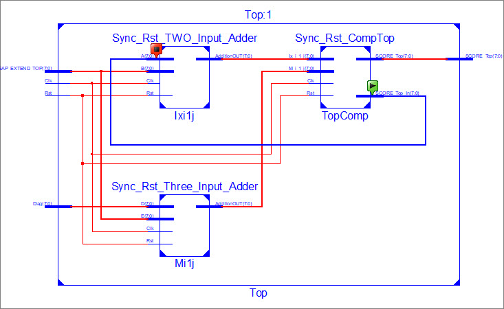
module Top(Clk,Rst,Diag,GAP_EXTEND_TOP,SCORE_Top,SCORE_Top_Out);
parameter ComputeDataWidth = 8;
input Clk,Rst;
input signed [ComputeDataWidth-1:0] Diag,GAP_EXTEND_TOP;
output signed [ComputeDataWidth-1:0] SCORE_Top,SCORE_Top_Out;
wire signed [ComputeDataWidth-1:0] TopM,TopIx,In;
Sync_Rst_Three_Input_Adder
#( .ComputeDataWidth (ComputeDataWidth))
Mi1j
( .Clk (Clk),
.Rst (Rst),
.D (Diag),
.E (GAP_EXTEND_TOP),
.AdditionOUT (TopM)
);
Sync_Rst_TWO_Input_Adder
#( .ComputeDataWidth (ComputeDataWidth))
Ixi1j
( .Clk (Clk),
.Rst (Rst),
.A (In),
.B (GAP_EXTEND_TOP),
.AdditionOUT (TopIx)
);
Sync_Rst_CompTop
#( .ComputeDataWidth (ComputeDataWidth))
TopComp
(
.Clk (Clk),
.Rst (Rst),
.M_i_1_j (TopM),
.Ix_i_1_j (TopIx),
.SCORE_Top (SCORE_Top),
.SCORE_Top_In (In),
.SCORE_Top_Out (SCORE_Top_Out)
);
endmodule
Three input adder
`timescale 1ns / 1ps
module Sync_Rst_Three_Input_Adder(Clk,Rst,D,E,AdditionOUT);
//Parameters must come here now until may
parameter ComputeDataWidth = 8;
parameter F = -12;
input Clk,Rst;
input signed [ComputeDataWidth-1:0] D,E;
output reg signed [ComputeDataWidth-1:0] AdditionOUT;
wire [ComputeDataWidth-1:0] PostAdd;
//Perform the addition
generate
begin : Adding
assign PostAdd = D + E + F;
end
endgenerate
always@(posedge Clk)
begin
if(Rst)
AdditionOUT <= 8'b0;
else
AdditionOUT <= PostAdd;
end
endmodule
Two input adder
`timescale 1ns / 1ps
module Sync_Rst_TWO_Input_Adder(Clk,Rst,A,B,AdditionOUT);
//Parameters must come here now until may
parameter ComputeDataWidth = 8;
input Clk,Rst;
input signed [ComputeDataWidth-1:0] A,B;
output reg signed [ComputeDataWidth-1:0] AdditionOUT;
wire [ComputeDataWidth-1:0] PostAdd;
//Perform the addition
generate
begin : Adding
assign PostAdd = A + B;
end
endgenerate
always@(posedge Clk)
begin
if(Rst)
AdditionOUT <= 8'b0;
else
AdditionOUT <= PostAdd;
end
endmodule
Comparator
`timescale 1ns / 1ps
module
Sync_Rst_CompTop(Clk,Rst,M_i_1_j,Ix_i_1_j,SCORE_Top,SCORE_Top_In,SCORE_T
op_Out);
//Parameters must come here now until may
parameter ComputeDataWidth = 8;
input Clk,Rst;
input signed [ComputeDataWidth-1:0] M_i_1_j,Ix_i_1_j;
output reg signed [ComputeDataWidth-1:0]
SCORE_Top,SCORE_Top_In,SCORE_Top_Out;
//Decode the results
always@(posedge Clk)
begin
if(Rst)
begin
SCORE_Top <= 8'b0;
end
else if (M_i_1_j > Ix_i_1_j)
begin
SCORE_Top <= M_i_1_j;
end
else
begin
SCORE_Top <= Ix_i_1_j;
end
end
always@*
begin
if(M_i_1_j > Ix_i_1_j)
begin
SCORE_Top_In <= M_i_1_j;
end
else
begin
SCORE_Top_In <= Ix_i_1_j;
end
end
always@*
begin
if(M_i_1_j > Ix_i_1_j)
begin
SCORE_Top_Out <= M_i_1_j;
end
else
begin
SCORE_Top_Out <= Ix_i_1_j;
end
end
endmodule
Hi again :-)

As I can see from the timing diagram, the output of the 2-input adder is
always 'X' even after the reset becomes active. In the 2-input adder you
have used a synchronous reset, i.e. the reset input is evaluated only at
a rising clock edge. In your simulation, however, there is no rising
clock edge while reset=1. Due to the feedback loop, the undefined state
will be kept forever. Try to keep reset=1 for at least 1 full clock
cycle in the simulation.

That is what I can see from the code. I hope this solves the problem,
otherwise I have to run the simulation here.

The other way would be to use an asynchronous reset (add Rst to the
sensitivity list of the always@ block). This way, the reset is evaluated
immediately whenever it occurs. For FPGA, however, sync reset is better
for timing, except if you have a safety critical system, that must be
resettable even if the clock stops from oscillating for some failure. I
think this is not the case for you, so stay with sync reset.

Why do you encapsulate the addition in an extra generate environment?
This is not wrong but not necessary. Generates are used only for
conditional code generation or in generate loops (as for the PE as we
discussed at the beginning).

Your code can be simplified:

...
always@(posedge Clk)
    begin
      if(Rst)
        AdditionOUT  <= 8'b0;
      else
        AdditionOUT  <= D + E + F;
    end
...

Regards
BTW, I noticed that the HDL code for 2- and 3-input adders are almost
identical except for the addition of constant parameter F. You could an
use the 3-input adder module also for 2-input addition by setting the F
parameter to 0 at instantiation: