Hello guys . I need your help .
I use code VGA in the FPGA PROTOTYPING
BY VERILOG EXAMPLES Book of Pong P. Chu to implement on kit de2-70
cyclone II Ep2c35f672c6 , but it doesn't work .... What's wrong ?
This is my code and pin assignment :
https://drive.google.com/file/d/1TPM6Eg-syR3MmesIT7idqWc7VEeycoYC/view
Thank guys !!!
Attached files:
-

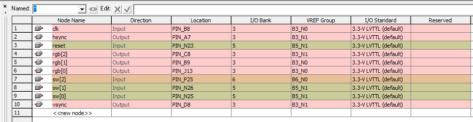
assiment.PNG
23 KB -

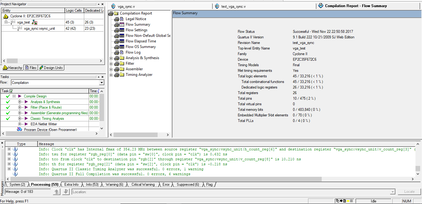
quatus.PNG
75 KB
sinhton wrote:
> This is my code
Pls attach your verilog files here as simple *.v files, then even I on
my mobile may be able to help...

> but it doesn't work .... What's wrong ?
What does not work? What error message do you get from which part of the
toolchain? Waht do you expect and what do you get instead? Does the
simulation of your design run fine?

> This is my code and pin assignment
Does the pin assignment match your hardware?
Did you simulate it ? normally you get quite a bit of information from
simulation. Not everyone has exactly the same board like you or the time
to try to modify what you wrote.
I find the amount of logic used as really small, 45 LUTs ? Maybe it only
generates a simple pattern...
Make a testbench to stimulate the clock and reset and see why it doesn't
work. If it works meaning vsync and hsync have the proper period and
polarity and you have some pixels to show... maybe the PINs are not
correctly set or the clock is routed to some other pin... there are may
possibilities... Do you have access to an oscilloscope ?
Maybe... did you have a look at what the code is supposed to do ?... I
think you may be missing some ahem "sw" input.
Attached files:
-

vgaa.PNG
440 KB
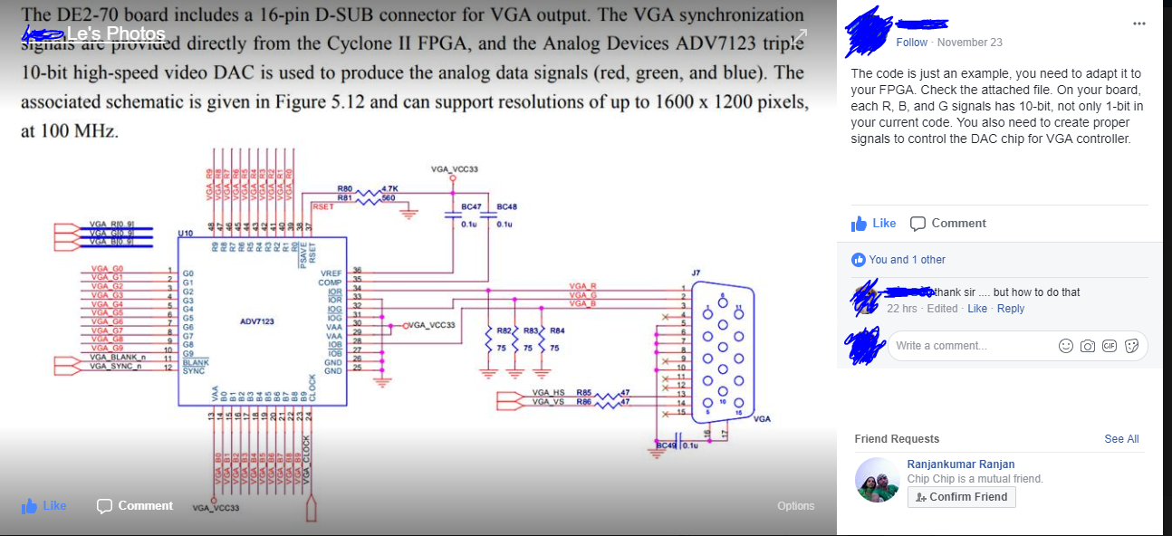
thank everyone ... but i am sure my code and my pin assignment are
correct ( i checked my pin assignment) ... i think the trouble is with
this picture ... but how to do it ??
Finally , i would like to know how  to use code in the book to implement
on kit de2-70 ... what do i need to change  ?
You could route your clock also to a Test-Output-Pin to check that it
arrives in the FPGA. Next check the sync signals as already mentioned
above. If they are ok generate a test-pattern as output to the 3 colors,
if that is also ok route the real data to the output pins.
Your SYNC-Signals are High-Active,
but they should be Lo-Active. The
rest looks ok.
i programmed fbga with xp2 lattice chip to switch lvds from IPU and GPU
on Macbook pro 15 2011. The screen resolution of 1440x900 and 1600x900
is good. but 1920x1200 results are bad. I think the data and clk channel
n and p output from the chip is not good. You let me ask how I write
code to ensure that clk and data out are good
peter wrote:
> I think the data and clk channel n and p output from the chip is not
> good.
Can you get a scope and do some measurements? That's way better than
guessing...


BTW: why don't you simply start a new thread for a completely new
question?
Please log in before posting. Registration is free and takes only a minute.
Existing account
Do you have a Google/GoogleMail account? No registration required!
Log in with Google account
Log in with Google account
No account? Register here.