I have made some code to perform this task but i see no out come on the
lcd.
my hardware is ok .can any one suggest a solution to this please.
Oldham P. wrote:
> I have made some code to perform this task but i see no out come on the
> lcd. my hardware is ok .

There is too much information at once, I cannot handle this.
It would be very helpful if you post at least your schematic.

595 pins 10 & 14 unconnected?
power? decoupling capacitors?
what is the connection between pin 7 and atmega good for?
pin 10 and 16 are high.

I don't know about pin 7 .this is my question too .but this is the
hardware
I already have.can not change it.
I just can guess that pin 37 of your AtMega is data out, which should go
to pin 14 at 74xx595 (serial data in).
Pin 7 could be connected to data in of another 74xx595, which isn't used
in your configuration.
Ok. Thanks.Now forgetting about pin7 ,what can be done about software?
incidentally this hardware works ok with another programmed ic atmega32,
but it dose not work with the one I have programmed.
Look, the information you're providing is extremely sparse. It is almost
impossible to help.

Nobody knows anything about the code you are running on the your atmega.
How do you expect anybody to be able to say something about software
then?

Also: are you having a data signal to the 74xx595 data in (pin 14) now?
Your "schematic" doesn't show it, and you didn't confirm so far.

It would be good if you start debugging on your side, like attaching a
scope or logic analyser and measuring some of the key signals (clk,
data, cs).

Another possibility is that there is a difference in the wiring between
the working system and the new one (wrong/missing signal connection).
Please verify.
Ok let me forward the code for your inspection.

(This code is written for a separate set up on bread board.)
I must apologize to you for bothering you on this.


#include <io.h>
#include <delay.h>
#include <mega32a.h>
/***************************************

Configure Connections

****************************************/

#define HC595_PORT   PORTA
#define HC595_DDR    DDRA

#define HC595_DS_POS PORTA.4      //Data pin (DS) pin location

#define HC595_SH_CP_POS PORTA.5      //Shift Clock (SH_CP) pin location
#define HC595_ST_CP_POS PORTA.6      //Store Clock (ST_CP) pin location

//#define LCD_DATA PORTA.4 // LCD data port
#define en PORTA.2 // enable signal
#define rw PORTA.1 // read/write signal
#define rs PORTA.0 // register select signal


/***************************************
Configure Connections ***ENDS***
****************************************/

//Initialize HC595 System

void HC595Init()
{
   //Make the Data(DS), Shift clock (SH_CP), Store Clock (ST_CP) lines
output
   //HC595_DDR|=((1<<HC595_SH_CP_POS)|(1<<HC595_ST_CP_POS)|(1<<HC595_DS_POS
));
   DDRA=0xff;
}


//Low level macros to change data (DS)lines
#define HC595DataHigh() (HC595_PORT|=(1<<HC595_DS_POS))

#define HC595DataLow() (HC595_PORT&=(~(1<<HC595_DS_POS)))

//Sends a clock pulse on SH_CP line
void HC595Pulse()
{
   //Pulse the Shift Clock

   //HC595_PORT|=(1<<HC595_SH_CP_POS);//HIGH
   PORTA.5=1;
   delay_ms(20);
   //HC595_PORT&=(~(1<<HC595_SH_CP_POS));//LOW
   PORTA.5=0;

}

//Sends a clock pulse on ST_CP line
void HC595Latch()
{
   //Pulse the Store Clock

   //HC595_PORT|=(1<<HC595_ST_CP_POS);//HIGH
   PORTA.6=1;
   delay_ms(10);
   PORTA.6=0;
   //HC595_PORT&=(~(1<<HC595_ST_CP_POS));//LOW
   delay_ms(10);
}


/*

Main High level function to write a single byte to
Output shift register 74HC595.

Arguments:
   single byte to write to the 74HC595 IC

Returns:
   NONE

Description:
   The byte is serially transfered to 74HC595
   and then latched. The byte is then available on
   output line Q0 to Q7 of the HC595 IC.

*/
//unsigned int data ;
void HC595Write(unsigned int data)
 {
   //Send each 8 bits serially
    int i=0;
   //Order is MSB first
   for(i=0;i<8;i++)
   {
      //Output the data on DS line according to the
      //Value of MSB
      if(data & 0b10000000)
      {
         //MSB is 1 so output high
         //HC595DataHigh();
         PORTA.4=1;
         delay_ms(1000);
      }
      else
      {
         //MSB is 0 so output high
         //HC595DataLow();
         PORTA.4=0;
         delay_ms(1000);
      }

      HC595Pulse();  //Pulse the Clock line
      delay_ms(1000);
      data=data<<1;  //Now bring next bit at MSB position
      delay_ms(1000);
   }

   //Now all 8 bits have been transferred to shift register
   //Move them to output latch at one
   HC595Latch();
   delay_ms(1000);
  }

/*

Simple Delay function approx 0.5 seconds

*/

void Wait()
{
int i=0;
   for(i=0;i<30;i++)
   {
      delay_ms(10);
   }
}
  int i=0;
 // uint_t data;     //Initialize HC595 system
void main()
{
 DDRB=0xff;
 PORTB=0xff;
 DDRA=0xff;
 PORTA=0xff;

  for(i=0;i<=3;i++) //Startup Led
  {
  PORTB.4=~PORTB.4;
  delay_ms(200);
  }
  PORTB.4=1;

    PORTA.7=0; //pin 13 595
  PORTA.1=0;   //w/r lcd
  PORTA.3=0;   //v0 lcd
  delay_ms(1000);
   HC595Init();
  // LCD init
   HC595Write(0x38);   //Write the data to HC595
         Wait();                 //Wait

  rs=0;rw=0;en=1; // RS and RW as LOW and EN as HIGH
    delay_ms(100);
   rs=0;rw=0;en=0;
   delay_ms(200);
    HC595Write(0x38);   //Write the data to HC595
         Wait();                 //Wait

  rs=0;rw=0;en=1; // RS and RW as LOW and EN as HIGH
    delay_ms(100);
   rs=0;rw=0;en=0;
   delay_ms(20);
    HC595Write(0x38);   //Write the data to HC595
         Wait();                 //Wait

  rs=0;rw=0;en=1; // RS and RW as LOW and EN as HIGH
    delay_ms(100);
   rs=0;rw=0;en=0;
   delay_ms(200);

   HC595Write(0x0f);   //Write the data to HC595
         Wait();                 //Wait

  rs=0;rw=0;en=1; // RS and RW as LOW and EN as HIGH
    delay_ms(100);
   rs=0;rw=0;en=0;
   delay_ms(200);
//  HC595Write(0x0f);   //Write the data to HC595
//         Wait();                 //Wait
//
//  rs=0;rw=0;en=1; // RS and RW as LOW and EN as HIGH
//    delay_ms(10);
//   rs=0;rw=0;en=0;
//   delay_ms(20);


   while(1)
   {
      PORTA.3=0;  // back light on/off
    delay_ms(1000);
         rs=1;rw=0;en=1; // RS and RW as LOW and EN as HIGH
    delay_ms(100);
         HC595Write(0b01010101) ; //Write the data to HC595
         Wait();                 //Wait

   rs=1;rw=0;en=0;
   delay_ms(200);
    rs=1;rw=0;en=1; // RS and RW as LOW and EN as HIGH
    delay_ms(100);
         HC595Write(0x32) ; //Write the data to HC595
         Wait();                 //Wait

   rs=1;rw=0;en=0;
   delay_ms(200);

//     rs=1;rw=0;en=1; // RS and RW as LOW and EN as HIGH
//    delay_ms(1000);
//         HC595Write(0x14) ;   //Write the data to HC595
//         Wait();                 //Wait
//
//   rs=1;rw=0;en=0;
//   delay_ms(20);
//    rs=1;rw=0;en=1; // RS and RW as LOW and EN as HIGH
//    delay_ms(10);
//         HC595Write(0xff) ;   //Write the data to HC595
//         Wait();                 //Wait
//
//   rs=1;rw=0;en=0;
//   delay_ms(20);
     PORTA.3=0;
    delay_ms(1000);


   }


}
Attached files:
-

595-to-display.png
97 KB
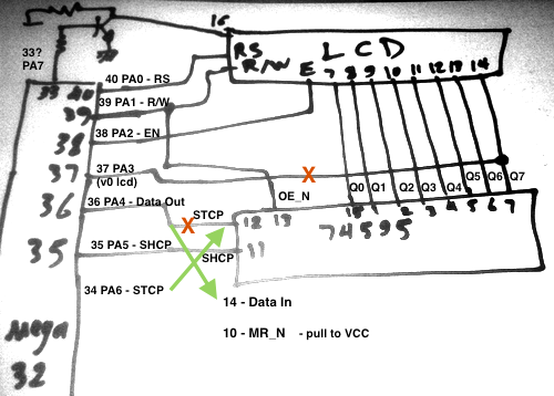
I think there is a mismatch of the port pins you are using in firmware
and the actual connections to your hardware. see attached picture.
Also verify the usage of PA3 and PA7 (if I read the "33" correctly in
the top left corner).
Sorry you are correct I did it wrongly  .In actual firmware it is as you
have drawn.
 problem is still on!
Oldham P. wrote:
> In actual firmware it is as you
> have drawn.

An what about the status of the actual hardware?
More specific: pin 14 - serial data in?
Yes pin 14 is for data and connected.More to say now I have come to a
state where the data is reaching to lcd (by connecting led and resistor
in place of lcd )but nothing is seen in lcd.Please see whats the bug!
Please provide an updated and complete schematic as well as the actual
and latest source code files you are using for this setup.

Btw: source code files could be uploaded as attachments here.
Attached files:
-

pic2.jpg
230 KB
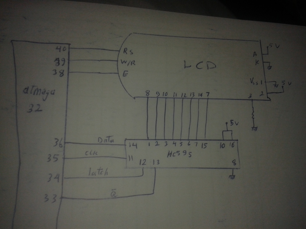
the case is :
I can send character to lcd ,but not numbers and I can not go to the
second line of lcd. More  over there is unwanted space between the
letters
my code is attached.
Please log in before posting. Registration is free and takes only a minute.
Existing account
Do you have a Google/GoogleMail account? No registration required!
Log in with Google account
Log in with Google account
No account? Register here.