

Hello everyone,

I tried to connected via SPI the ADC from Analog device, AD7176 and an
the Evalution Board Nexys 4 from Digilent.
The Problem is that I need to decouple the MISO pin to ground with an
220pF capacitance so that it works !!!!

To test the SPI communication (10MHz), I attempt to read the
ID-register.
I tied the CS to ground because I just want to read 1 AD.
When I disconnect the MISO form the FPGA the ADC gives me a good ID
Signal, so the clock and the MOSI signal are OK.
But when I connect it to the FPGA I need this capacitance so that the
signal good is.
the Signal clk and MISO are represented without capacitance in NewFile0
and with the Capacitance in NewFile1.

The IO-pin from the FPGA are with an Zener Diode protected!  does
somebody have an Idea if this zener diode a problem is for the AD7176?
Does someone have experience with it?


Thanks a lot!

David
Attached files:
-

NewFile0.png
3.7 KB -

NewFile0.png
3.7 KB -

NewFile1.png
3.4 KB
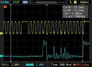
Hi David,

you did not explain the PNGs. I guess, the first and the second ones are
accidentally identical and the third one is when the AD's output is
disconnected from the FPGA.

In this case I would bet that your FPGA output is enabled to Gnd just
after the fist '1' from the AD has been sent. This is why you see only
the 3 leading slopes of the succeeding '1's.

But I don't have an idea why this is solved with the capacitor.

Much luck!
Hi Uwe Beis,

for the PNGs, the NewFile0.png respresent the CLK and MISO when the AD
is connected to the FPGA without the capacitor and the NewFile1.png
respresent the CLK and MISO when the AD is connected to the FPGA with
the capacitor.

Uwe Beis wrote:
> In this case I would bet that your FPGA output is enabled to Gnd just
> after the fist '1' from the AD has been sent. This is why you see only
> the 3 leading slopes of the succeeding '1's.

Are you meaning that the FPGA tied the MISO signal to ground?

Thanks a lot
David M. wrote:
> Are you meaning that the FPGA tied the MISO signal to ground?

Yes, that's what I meant. But ignore the next paragraphs I wrote here,
I'm sure the answer is explained in my last paragraph.

It doesn't sound plausible that a pin that is configured as an input
suddenly becomes an output and that that can be avoided by 220pF. But
the spikes look so typical for a signal that is probed at the source
(the AD) when high is emitted, runs to the sink, is shorted there and
runs back to the source again tying it to Gnd. On the other hand the
spike is 20 ns long, that would mean 2 x 10 ns run time which equals to
a few meters of cable length - and that's not plausible any more :-(

No I'm not that sure that the FPGA constantly turns the output on. But
maybe with each rising edge, except for the first one - but why during
a double high, too? Well, should I be asked to program such a behaviour
I think I would know, how to.

You could insert a resistor at the AD's output, about 100 Ohms, and
maybe the effect vanishes, too. But of course it is important to know
the cause, and not only a remedy that happens to work.

I presume that your tracks are not too long, ground is massive and VCC
is equipped with enough 100 nF.

One more idea: Insert 10 Ohms and, in case the effect is still there,
look whether the FPGA really shortens the signal (voltage across 10
Ohms) or not (no voltage across 10 Ohms). In the latter case the AD
would abort it's transmission of a high.

And there is the next and ultimate idea: When you have a crosstalk from
MISO to CLK than the AD generates with (almost?) each rising MISO edge
another clock spike and immediately (i.e., 20 ns later) continues with
the next bit. And having another close look this theory really matches
your oscillograms exactly. And it explains the 220 pF. Yes, that's it!
The shown signals are crap. Either the scope is crap to start with, or
the GND leads of the scope are not properly connected, or the layout is
"improvable"
Could you show us the layout ? and perhaps a picture of your measurement
setup?
Hy Uwe Beis,

Thanks for the explanations but I don't understand how I can solve my
problem!

Regards
Hi Siebzehn Für Fuenfzehn,


here the layout!
the photo of the setup will follow

regards
David M. wrote:
> how I can solve my problem!
Except some general rules I  cannot tell you much, particularly because
I don't know the means and possibilities you have. Also I cannot open
.brd and .sch files. Maybe 17-4-15 can help more.

1. To keep the tracks as short as possible and as far as possible away
from each other is a common advice, but it is nonsense: "As short (far)
as" is no rule and, in case, "as short (far) as" may still be much too
long (close). On the other hand: Your tracks are obviosly either to lond
and/or too close to each other. I would say: The tracks need to
sufficiently short and sufficiently far away from each other

2. A good practice is always to add a series resistor to the outputs of
fast sources, again close to the pin. This resistor helps to avoid
reflections, over- and undershoots and high frequency resonances (->
EMC). The resistance should match the impedance of the tracks. I use for
dual sided PCBs about 100 Ohms and for multilayer PCBs 33 to 68 Ohms.

Maybe these resistors, one for the MISO close to the AD, one for Clk,
close to the FPGA (and MOSI, CS and much more), would already solve the
problem. But if so, you never would know whether this solution just
happens to be sufficient at your sample or if it is really far enough on
the safe side.

Of course you need solid a ground layer and well decoupled VCC pins.
Please log in before posting. Registration is free and takes only a minute.
Existing account
Do you have a Google/GoogleMail account? No registration required!
Log in with Google account
Log in with Google account
No account? Register here.