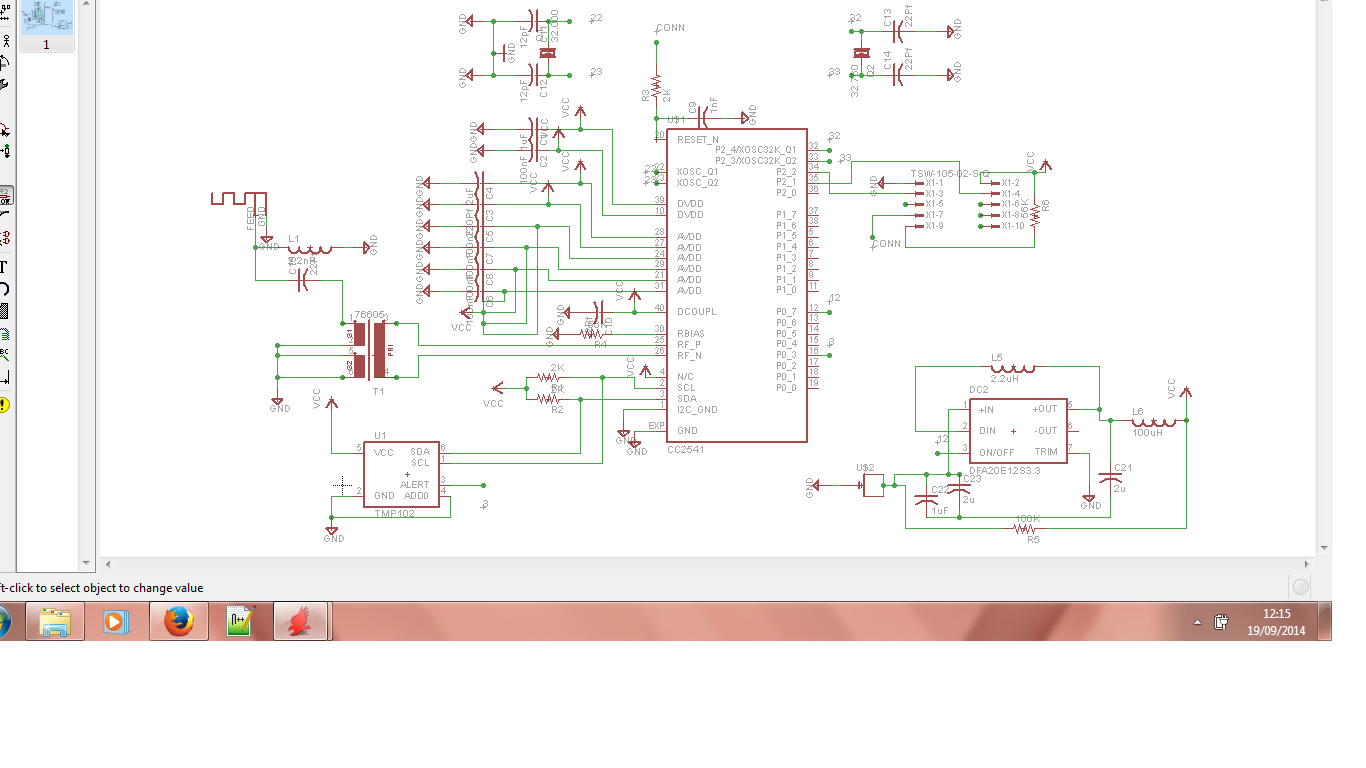
Hello all,

I am doing a project where I have to design a PCB. I am new in this
field. I am using EAGLE PCB software.


About my project: I am working on a project where I have to measure the
environments temperature. I am using TI's CC2541 Bluetooth soc, temp
sensor TMP102, DC DC convertor, SOC debug flash TSW-105-02-S-Q and
MURATA's Balun transformer. Whenever I put the battery in my PCB, the
temp sensor reads the data and send it to my phone via Bluetooth. For
this PCB design I am using eagle software. Since I am new to this
software and I am working alone in this project I want help from you
all.


Till now I have the schematic design on software. I am attaching my pdf
file here, so you guys check the file and tell me if I am going in a
right direction or not?

And also how to check the design if it is correct or not? I clicked on
the error button, it is showing warnings only not an error.

guys can you help me with this?
Attached files:
-

12.png
71 KB
If you are new to the subject of circuit design, a RF design is hard to
do. You should have a look at the TI reference design here:

http://www.ti.com/tool/cc2541sensortag-rd

They are using a 4 layer PCB. If you want a working board I would
suggest to copy schematic and design and add your special requirements
to design and board. You should not change the RF part of the layout.

Greetings from Germany

Einhart
I am using the same ti sensor board diagram....i haven't changed
anything...I just copy that circuit and made to my requirement....just
check my diagram once more...the rf part is the same as sensor tag....
Hello,

Dushyant Kumar SIngh wrote:
> I am using the same ti sensor board diagram....i haven't changed
> anything...I just copy that circuit and made to my requirement....just
> check my diagram once more...the rf part is the same as sensor tag....

Einhart doesn't refer to your schematic. He is talking about the pcb
layout.

Best regards
Guido
Please log in before posting. Registration is free and takes only a minute.
Existing account
Do you have a Google/GoogleMail account? No registration required!
Log in with Google account
Log in with Google account
No account? Register here.