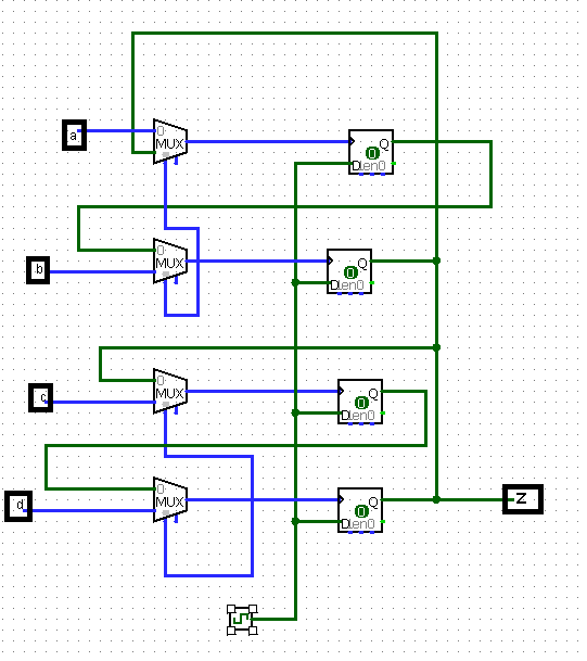
Communication system: Interleaver

OP #3808335
Rate this post
useful
not useful
Hey! I have been stuck on this exercise for a few days and i have 
realized that i wont make it on my own. So i decided to ask here for 
help! :)

 In a Communication system we want to interleave four inputs signals, 
a,b,c and d coming from different antennas, ( See the attached picture). 
Each input provides a valid data every four clock cycles. This is 
indicated by a data_temp input. This signal is used as a control signal 
and its value is ‘1’ during one clock cycle every four clock cycles.

a)  Design(draw) a circuit that interleaves the four inputs signals. 
Distinguish between the path for data and the control logic. You do not 
need to specify the word lenth of the signals unless it is relevant for 
understanding the circuit.
Attached files:
Moderator (Company: Titel) #3808416
Rate this post
useful
not useful
Rob Griffin wrote:
> that i wont make it on my own
Does "wont" mean "want" or "won't". Both cases are possible...

> Design (draw) a circuit that interleaves the four inputs signals.
What part of this particular task is related to FPGA or Verilog or VHDL? 
Look for components named "serializer" or "parallel to serial 
converter".

> So i decided to ask here for help! :)
And whats the question? Where's your problem? How much of your homework 
did you do already?
OP #3808436
Rate this post
useful
not useful
Lothar Miller wrote:
> Rob Griffin wrote:
>> that i wont make it on my own
> Does "wont" mean "want" or "won't". Both cases are possible...
>
>> Design (draw) a circuit that interleaves the four inputs signals.
> What part of this particular task is related to FPGA or Verilog or VHDL?
> Look for components named "serializer" or "parallel to serial
> converter".
>
>> So i decided to ask here for help! :)
> And whats the question? Where's your problem? How much of your homework
> did you do already?


I meant "won't" I'm sorry for that. My question is

"Design(draw) a circuit that interleaves the four inputs signals.
Distinguish between the path for data and the control logic. You do not
need to specify the word lenth of the signals unless it is relevant for
understanding the circuit."

And yes it is related to FPGA and VHDL because when I have my circuit i 
will code it in VHDL then program it on my FPGA.
Guest #3808447
Rate this post
useful
not useful
You will need a multipexer at 4 times the speed of the incoming data, a 
data buffer, since all the 4 signals seem to occur simultaneously and a 
counter controlling the multiplexer address, being syched with the 
buffer enable
Moderator (Company: Titel) #3808459
Rate this post
useful
not useful
Rob Griffin wrote:
> My question is
Isn't a question that thing with an question mark at its end?

However: did you do a little google search for the keywords I gave you? 
And did you do a look for e.g. the 74165? Or have a look for the inside 
schematic of this serializer: 
http://www.micrel.com/index.php/en/products/clock-timing/clock-data-distribution/mux-demux/article/4-sy10100e446.html

> And yes it is related to FPGA and VHDL
Indeed this task here is in no way related to any HDL. Its pure 
analyzing and schematic...

Reply

Please log in before posting.

or

Log in with Google account

Registration is free and takes only a minute.

Register now