EmbDev.net

Forum: FPGA, VHDL & Verilog Poor RTL optimization


von Kurt E. (Company: RPI) (khenglish)


Attached files:

Rate this post
useful
not useful
So my Verilog file for an asynchronous bi-directional memory mostly 
works, but it has some problems.

1.  The layout is EXTREMELY inefficient, which can be seen in the RTL 
viewer.  There is a 3-input AND-gate at the enable of every memory bit. 
This AND-gate has the same identical inputs for every memory bit.  Every 
single one of these AND-gates could be eliminated since the memory 
latches are never supposed to be disabled.  Fixing this would probably 
cut FPGA usage by over 50%.

2. The READY signal is at times undefined.  It should never be 
undefined.  How can I fix this?

3. I can't get else statements to work.  When trying to use them I 
always get a memory initialization error when compiling.

Below is the Verilog.  In the screenshot I also have the timing diagram.
1
module sysmem (
2
A,
3
WR,
4
D,
5
READY
6
);
7
8
//input ports
9
input [15:0] A;
10
input WR;
11
12
//output ports
13
inout [7:0] D;
14
output READY;
15
16
//registers/wires
17
reg [7:0] Dout;
18
reg [7:0] memdat [0:255];
19
reg READY;
20
21
initial begin
22
  $readmemh("sysinit.txt", memdat);
23
end
24
25
assign D = (WR) ? Dout : 8'bz;
26
27
always @ (*)
28
  begin
29
    begin: rdyset
30
      if (memdat[A] == D)
31
        READY = 1'b1;
32
      if (memdat[A] != D)
33
        READY = 1'b0;
34
    end
35
    begin: memread
36
      if (WR)
37
        Dout = memdat[A];
38
    end
39
    begin: memwrite
40
      if (!WR)
41
        memdat[A] = D;
42
    end
43
  end
44
endmodule

: Edited by Moderator
von Lothar M. (Company: Titel) (lkmiller) (Moderator)


Rate this post
useful
not useful
Kurt English wrote:
> There is a 3-input AND-gate at the enable of every memory bit.
Where?

> FPGA
Which one and what toolchain do you use?

> Fixing this would probably cut FPGA usage by over 50%.
You should use one of the synchronous ram blocks. That would be the most 
efficient way to implement memory ON a FPGA.

Your cannot use your ram the way you did it in the timing diagram in 
real life!
Enabling the write signal all over the time will cause spurious writes 
to any memory register due to glitches in the adress lines. You must 
have any kind of enable signal to tell your ram that now data and 
adress are valid.
Just have a look at the data sheet of some discrete asynchronous rams.

BTW: Pls wrap your code in the code tags
1
   [c]
2
     your code
3
   [/c]

: Edited by Moderator
von Kurt E. (Company: RPI) (khenglish)


Rate this post
useful
not useful
Fixed it.  Adding a buffer instead of directly accessing the memory got 
rid of the hundreds of extra inferred latches.  READY was screwed up due 
to the testing schematic trying to write to the D bus the same time the 
memory was writing to it.
1
module sysmem (
2
A,
3
WR,
4
D,
5
READY
6
);
7
8
//input ports
9
input [15:0] A;
10
input WR;
11
12
//output ports
13
inout [7:0] D;
14
output READY;
15
16
//registers/wires
17
reg [7:0] Dout;
18
reg [7:0] memdat [0:255];
19
reg READY;
20
reg [7:0] membuf;
21
22
initial begin
23
  $readmemh("sysinit.txt", memdat);
24
end
25
26
assign D = (WR) ? Dout : 8'bz;
27
28
always @ (A or D or WR)
29
  begin
30
  membuf = memdat[A];
31
    begin: rdyset
32
      if (membuf == D)
33
        READY = 1'b1;
34
      else if (membuf != D)
35
        READY = 1'b0;
36
      else
37
        READY = 1'b0;
38
    end
39
  end
40
always @ (A)
41
  begin
42
    begin: memread
43
      Dout = memdat[A];
44
    end
45
  end
46
always @ (posedge WR)
47
  begin
48
    begin: memwrite
49
      memdat[A] = D;
50
    end
51
  end
52
endmodule

von Lothar M. (Company: Titel) (lkmiller) (Moderator)


Rate this post
useful
not useful
Its slightly more complex.
This code implements latches (which is usually not a good idea or 
practice):
1
always @ (*)
2
  begin
3
    begin: memwrite
4
      if (!WR)
5
        memdat[A] = D;
6
    end
7
  end

And the "new" code implements flipflops
1
always @ (posedge WR)
2
  begin
3
    begin: memwrite
4
      memdat[A] = D;
5
    end
6
  end

But keep in mind: you added one clock domain to your design. This may be 
not reproducable sync to your master clock!

von Kurt E. (Company: RPI) (khenglish)


Rate this post
useful
not useful
Lothar Miller wrote:

> But keep in mind: you added one clock domain to your design. This may be
> not reproducable sync to your master clock!

Yeah I'm not sure how the CPU handles WR timing or when it checks the 
READY flag yet.  Definitely going to have to look it up and make sure 
what I did works.  I don't think the READY flag is still quite right, 
but it may be good enough to work.  Since I have to write the CPU 
microcode I'll figure it out then :)

Also to answer your earlier questions this is on an old Cyclone II FPGA. 
I cannot use the memory tool in Quartus because it does not work for 
asynchronous memory on the Cyclone 2, while memory implemented directly 
in VHDL or Verilog works fine.  The other big reason is because the 
Verilog needs to be portable so that another group member can place and 
route in Cadence to simulate a fab'd chip (simulating an 8080, possibly 
a Z80 for a final course project).

Thanks for your help!

von Kurt E. (Company: RPI) (khenglish)


Attached files:

Rate this post
useful
not useful
So it turns out that despite having a better looking RTL the memory is 
still using an exorbitant amount of FPGA area.  I made another memory 
that's simpler (not writable) but is 7 times larger (56bit word size) 
and it takes 1/8th the FPGA logic.
1
module sysmem (
2
A,
3
WR,
4
D,
5
READY
6
);
7
8
//input ports
9
input [7:0] A;
10
input WR;
11
12
//output ports
13
inout [7:0] D;
14
output READY;
15
16
//registers/wires
17
reg [7:0] Dout;
18
reg [7:0] memdat [0:127];
19
reg READY;
20
reg [7:0] membuf;
21
22
initial begin
23
  $readmemh("sysinit.txt", memdat);
24
end
25
26
assign D = (WR) ? Dout : 8'bz;
27
28
always @ (*)
29
  begin
30
31
  membuf = memdat[A];
32
    begin: rdyset
33
      if (membuf == D)
34
        READY = 1'b1;
35
      else
36
        READY = 1'b0;
37
    end
38
  end
39
always @ (A)
40
  begin
41
    begin: memread
42
      Dout = memdat[A];
43
    end
44
  end
45
always @ (posedge WR)
46
  begin
47
    begin: memwrite
48
      memdat[A] = D;
49
    end
50
  end
51
endmodule

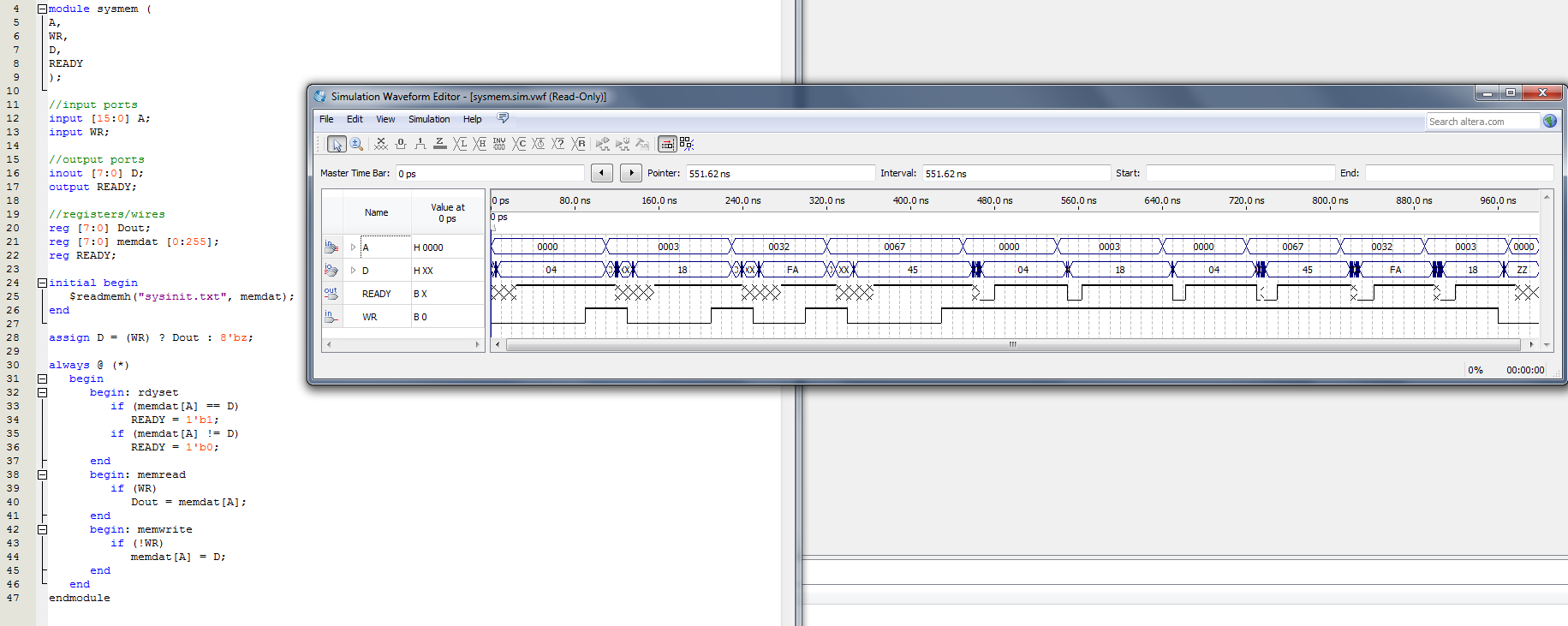
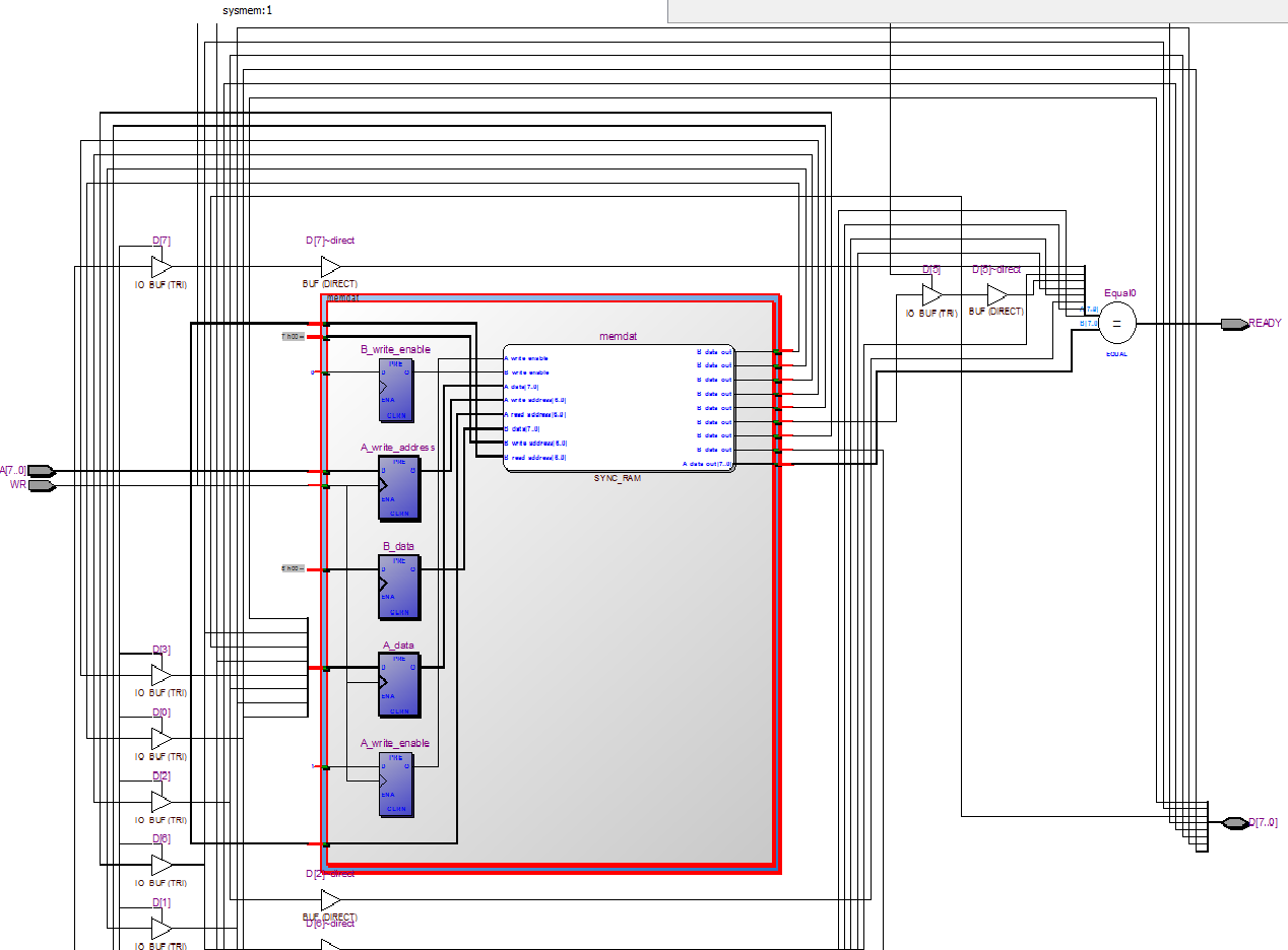
I shrank the memory size so it would compile faster.  Also for some 
reason this is compiling into a dual port memory.  Not sure why.  A 
screenshot of the RTL is attached.

If you know how to make the memory take less area I'd like to hear it.

Please log in before posting. Registration is free and takes only a minute.
Existing account
Do you have a Google/GoogleMail account? No registration required!
Log in with Google account
No account? Register here.