Hi all,
I need to design a decoder with the folling input and output:

input : AA0BB2CDFF1
output : AABBBBCDFFF

please help me if anyone has any idea of how to do this. Assume the
input data are stored in BRAM. I am not getting any idea of reading
consequtive data fromthe BRAM then compare the two data and depending on
the comparison result next address is raed as count. please help...
For future readers of this thread:
We come from http://embdev.net/topic/240164

> input : AA0BB2CDFF1
How do you distinguish between data and a lenght information?
"Numbers" and "Letters"?
A "Number" is repeat information, a "Letter" is data?

If Yes: do you know anything about hexadecimal values?
There 'A' is also a number as '9'...

> Assume the input data are stored in BRAM.
And where does it go after the computation? Do you just want to generate
a serial stream? Or must the result be stored in a RAM afterwards?
Thanks!

I am showing you the HEX file and its encoded format to make you
understand my problem:

Decoded Data: AA 00 FF FF FF 00 00 00 AA AA FF FF FF FF FF
encoded Data : AA 00 FF FF 01 00 00 01 AA AA 00 FF FF 03

when ever two consequtive data bytes are same then the next byte will be
read as the length of the bytes.


>And where does it go after the computation?
I want to to get serial stream of data  to the output. but input data
should come from a BRAM.

please help!!
Attached files:
-

RLD_1.gif
6.5 KB
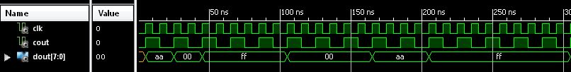
> when ever two consequtive data bytes are same
> then the next byte will be read as the length of the bytes.
enc: AA AA 00 FF FF
dec: AA AA FF FF
This is a little bit tricky, because here you have to "skip" one
cycle...

So, you can output Data with half the clock rate.
Or you can generate a "valid" signal parallel to the output data.
Or you can generate a clock signal that "clocks" out valid data (with
half the clock rate).

Here a solution for the 3rd way:
1 | -- decoded Data: AA 00 FF FF FF 00 00 00 AA AA FF FF FF FF FF
|
2 | -- encoded Data: AA 00 FF FF 01 00 00 01 AA AA 00 FF FF 03
|
3 | -- when ever two consequtive data bytes are same
|
4 | -- then the next byte will be read as the length of the bytes.
|
5 | library IEEE; |
6 | use IEEE.STD_LOGIC_1164.ALL; |
7 | use IEEE.NUMERIC_STD.ALL; |
8 | |
9 | entity RLD is |
10 | Port ( clk : in STD_LOGIC; |
11 | cout : out STD_LOGIC; |
12 | lastut : out STD_LOGIC_VECTOR(7 lastwnto 0)); |
13 | end RLD; |
14 | |
15 | architecture Behavioral of RLD is |
16 | type RAM_t is array (0 to 15) of std_logic_vector (7 lastwnto 0); |
17 | signal RAM : RAM_t := ( x"AA", x"00", x"FF", x"FF", x"01", x"00", x"00", x"01", x"AA", x"AA", x"00", x"FF", x"FF", x"03", others=>x"00"); |
18 | signal idx : integer range RAM_t'range := 0; |
19 | signal rpt : integer range 0 to 255; -- repeat counter max. 255 |
20 | signal last : std_logic_vector(7 lastwnto 0) := x"FF"; -- for lastuble-byte check: beware the first byte in RAM being xff! |
21 | signal gl : std_logic := '0'; -- get length out of RAM |
22 | signal phase : std_logic := '0'; |
23 | begin
|
24 | |
25 | process begin |
26 | wait until rising_edge(clk); |
27 | phase <= not phase; |
28 | if (phase='0') then |
29 | if (rpt>0) then -- something to repeat? |
30 | rpt <= rpt-1; |
31 | else
|
32 | idx <= idx+1; -- beware of reaching the end of the RAM! |
33 | if (last=RAM(idx)) then -- next: get length |
34 | gl <= '1'; |
35 | else
|
36 | last <= RAM(idx); |
37 | end if; |
38 | end if; |
39 | else
|
40 | if (gl='1') then -- get length |
41 | rpt <= to_integer(unsigned(RAM(idx))); |
42 | idx <= idx+1; -- beware of reaching the end of the RAM! |
43 | end if; |
44 | gl <= '0'; |
45 | end if; |
46 | end process; |
47 | |
48 | lastut <= last; |
49 | cout <= phase; |
50 | |
51 | end Behavioral; |
Result: see screenshot.
Attached files:
-

RLD_valid.gif
5.6 KB
> Thanks a lot Lother Miller !
De nada.
Just a little remark: replace the "lastwnto" with "downto". It was a
search and replace lapse... :-/
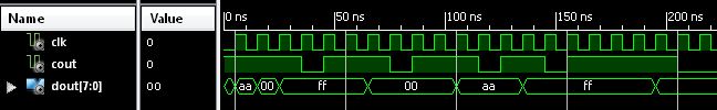
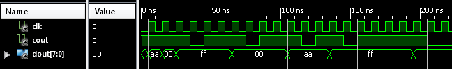
But my style would be the second one: generate a valid signal in
parallel to the clock and the data.1 | -- decoded Data: AA 00 FF FF FF 00 00 00 AA AA FF FF FF FF FF
|
2 | -- encoded Data: AA 00 FF FF 01 00 00 01 AA AA 00 FF FF 03
|
3 | -- when ever two consequtive data bytes are same
|
4 | -- then the next byte will be read as the length of the bytes.
|
5 | library IEEE; |
6 | use IEEE.STD_LOGIC_1164.ALL; |
7 | use IEEE.NUMERIC_STD.ALL; |
8 | |
9 | entity RLD is |
10 | Port ( clk : in STD_LOGIC; |
11 | cout : out STD_LOGIC; |
12 | dout : out STD_LOGIC_VECTOR(7 downto 0)); |
13 | end RLD; |
14 | |
15 | architecture Behavioral of RLD is |
16 | type RAM_t is array (0 to 15) of std_logic_vector (7 downto 0); |
17 | signal RAM : RAM_t := ( x"AA", x"00", x"FF", x"FF", x"01", x"00", x"00", x"01", x"AA", x"AA", x"00", x"FF", x"FF", x"03", others=>x"00"); |
18 | signal idx : integer range RAM_t'range := 0; |
19 | signal rpt : integer range 0 to 255; -- repeat counter max. 255 |
20 | signal last : std_logic_vector(7 downto 0) := x"FF"; -- for lastuble-byte check: beware the first byte in RAM being xff! |
21 | signal valid : std_logic := '1'; |
22 | begin
|
23 | |
24 | process begin |
25 | wait until rising_edge(clk); |
26 | if (rpt>0) then -- something to repeat? |
27 | rpt <= rpt-1; |
28 | valid <= '1'; |
29 | else
|
30 | idx <= idx+1; |
31 | if (idx<15) then |
32 | if (valid='0') then -- get length |
33 | rpt <= to_integer(unsigned(RAM(idx))); |
34 | valid <= '1'; |
35 | else
|
36 | if (last=RAM(idx)) then -- next: get length |
37 | valid <= '0'; |
38 | else
|
39 | last <= RAM(idx); |
40 | end if; |
41 | end if; |
42 | else
|
43 | valid <= '0'; |
44 | end if; |
45 | end if; |
46 | end process; |
47 | |
48 | dout <= last; |
49 | cout <= valid; |
50 | -- cout <= valid and clk; -- just for debugging: one pulse per byte
|
51 | end Behavioral; |
In the screenshot you must look at the rising edges of the clock an the
signal values before that. Those two belong togehter.
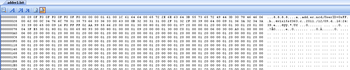
Hi Miller,
 I want to load data to the RAM from a file.I tried what you have
suggested(google transtate the code) but the code is not working. please
help me how to read the attached file and store data into the RAM to
simulate the program you gave me. Please help!!
Attached files:
-

adderbit.png
11 KB
> please help me how to read the attached file and store data into the RAM
> to simulate the program you gave me. Please help!!
Where does this file come from?
Is it a bit stream for a fpga (looks like), or what?
And what do you want with this bitstream in a RAM?
Yes,
it is a compressed bitstream for FPGA. I have compressed this file to
the adder1.bit, now I want to see the simulation result using the code u
gave that it is giving out the same bitstream from which I have
compressed.How can i do that?
how can I load the file to simulate the program? please help
> how can I load the file to simulate the program?
What you can simulate is a HDL description or a timing model of your
fpga design. But you cannot simulate a bitstream file. Thats a file that
must be loaded into a FPGA by a programming cable or something
similar...
Hi lother,
How can I know that what will be the no of clock cycle the decompressor
is taking to decompress the data if my input data is large? is their any
relation between the decoded/encoded data and the clock cycle?
> How can I know that what will be the no of clock cycle the decompressor
> is taking to decompress the data if my input data is large?
Even if the input data is "short" you cannot know the final length
until its decompressed. But a calculation of the final length could be
done with less clock cycles. Its just stepping through the ram and
adding the bytes and the "repeat" values.

> is their any
> relation between the decoded/encoded data and the clock cycle?
I do not understand this question...  :-/
Its a synchronous design, and so for sure there is a relation to the
clock. What other relation do you expect?
Hi,

I got that answer for my previous question but I am stuck with another
problem. is your code synthesizable ? it is giving a warnnin that Signal
'RAM' is not connected in block 'RLD' ties to its initial value.
and when I am going to systhesize the code It is showing No
combinational path delay. Is the code is not synthesizable?
In simulator there is an error coming:
ERROR: Index 16 out of bound 0 to 15.
ERROR: In process decoder.vhd:17

please help
> is your code synthesizable ?
With Xilinx XST it is.

> and when I am going to systhesize the code It is showing No
> combinational path delay.
Do you know what a combinational path delay is?
There is no combinational path in that design, because there is no path
between an input pin and an output pin.

> In simulator there is an error coming:
> ERROR: Index 16 out of bound 0 to 15.
Ahm....... as far as I see, that message is correct.
But why does it occur? Did you figure that out? Did you see the comment
I wrote there:
1 | idx <= idx+1; -- beware of reaching the end of the RAM! |
Just do a little of work by yourself and (at least) try to
understand what I did, then what you are doing, and then think about
such comments and corresponding error messages.
Lothar Miller wrote:
> Just do a little of work by yourself...

...or this thread will be closed. It is commendable that Lothar is
putting so much effort into helping others, but I do not like that
people think this is a place to get their homework done with no effort
of their own.