We have a pcb design with track space less than 5/5mil.
And i was told many fab can not make it,it will take long time to change
it.
Anyone have recommendation of fab who can produce it?
Attached files:
-

1.jpg
110 KB
Arkus B. wrote:
> We have a pcb design with track space less than 5/5mil.
Why the heck? I see plenty of empty space... :-/

> Anyone have recommendation of fab who can produce it?
https://www.multi-circuit-boards.eu/en/index.html -->
https://www.multi-circuit-boards.eu/en/products/printed-circuit-boards/special-production.html

https://www.wedirekt.de/en/ -->
https://www.wedirekt.de/web/media/16_wedirekt/spezifikationen/auswahlmoeglichkeiten/WEdirekt_-_Overview_of_the_ordering_options_2017.pdf
In short: almost every up-to-date fab is able to handle those
structures. But you will have to pay them for.
:
Edited by Moderator
@Arkus Bruce (Company: electronic lab) (arkusbruce001)

>We have a pcb design with track space less than 5/5mil.

Bad.

>And i was told many fab can not make it,it will take long time to change
>it.


I doubt it, especially in the screenshot shown. I guess you are just too
lazy.

Most manufacturer make 6/6 mil desgins using their standard process.
Smaller track/gap is (much) more expensive.

So your time to fix the design saves Money and provides a good
opportunity to improve your layout skills.

Njoy
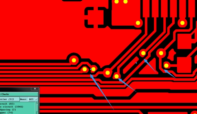
Arkus B. wrote:
> We have a pcb design with track space less than 5/5mil.

This is not the only problem with your design. There are many
unacceptable Errors even in this small Picture. I would refuse to
produce such PCBs in any case.

Georg
Just have look at the lower left corner, there is a window with a LOT of
error messeages . . .
Hi Njoy thank you for your suggestion, sound good idea.

i'll make some changes before manufacturing to save money.
Arkus B. wrote:
> i'll make some changes before manufacturing to save money.
And then run a DRC (design rule check) with real world parameters from a
manufacturer. When you go out of that DRC with no errors, then you are
ready for manufacturing.
:
Edited by Moderator
Attached files:
-

PCB-Prototype.png
60 KB
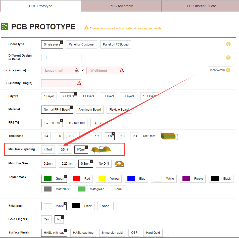
I have a Min Track/Spacing 4 / 4mil project produced at PCBGOGO. But the
price of this line spacing is very expensive. It is recommended to
modify your PCB design file. This will save you a lot of project costs.
:
Edited by User
For people, who also try to design with dense routings, the file found
under the link might be an interesting lecture. Conclusion for one part:
do not push to the manufacturer's boarders without any need.
https://resources.ema-eda.com/pcb-design-content-central/hitchhikers-guide-to-pcb-design
Please log in before posting. Registration is free and takes only a minute.
Existing account
Do you have a Google/GoogleMail account? No registration required!
Log in with Google account
Log in with Google account
No account? Register here.