hello i want to implement spi betwwen 2 fpga for nexys3 .. the first
board will be master the second will be slave so can these code do it ?
and what about the ucf ?

if not can u help me with the code and speacilly with ucf for master and
slave
this the ucf for spi_loopback

#Created by Constraints Editor (xc6slx45t-csg484-3) - 2011/06/08
NET "m_spi_2x_clk_i" TNM_NET = m_spi_2x_clk_i;
TIMESPEC TS_m_spi_2x_clk_i = PERIOD "m_spi_2x_clk_i" 15 ns HIGH 50%;
NET "s_clk_i" TNM_NET = s_clk_i;
TIMESPEC TS_s_clk_i = PERIOD "s_clk_i" 8 ns HIGH 50%;
#Created by Constraints Editor (xc6slx45t-csg484-3) - 2011/06/08
NET "m_clk_i" TNM_NET = m_clk_i;
TIMESPEC TS_m_clk_i = PERIOD "m_clk_i" 8 ns HIGH 50%;
NET "s_spi_sck_i" TNM_NET = s_spi_sck_i;
TIMESPEC TS_s_spi_sck_i = PERIOD "s_spi_sck_i" 30 ns HIGH 50%;
NET "m_spi_sck_o_OBUF" TNM_NET = m_spi_sck_o_OBUF;
TIMESPEC TS_m_spi_sck_o_OBUF = PERIOD "m_spi_sck_o_OBUF" 30 ns HIGH 50%;
NET "Inst_spi_master/core_n_clk" TNM_NET = Inst_spi_master/core_n_clk;
TIMESPEC TS_Inst_spi_master_core_n_clk = PERIOD
"Inst_spi_master/core_n_clk" 30 ns HIGH 50%;
INST "m_di_i<0>" TNM = m_di;
INST "m_di_i<1>" TNM = m_di;
INST "m_di_i<2>" TNM = m_di;
INST "m_di_i<3>" TNM = m_di;
INST "m_di_i<4>" TNM = m_di;
INST "m_di_i<5>" TNM = m_di;
INST "m_di_i<6>" TNM = m_di;
INST "m_di_i<7>" TNM = m_di;
INST "m_di_i<8>" TNM = m_di;
INST "m_di_i<9>" TNM = m_di;
INST "m_di_i<10>" TNM = m_di;
INST "m_di_i<11>" TNM = m_di;
INST "m_di_i<12>" TNM = m_di;
INST "m_di_i<13>" TNM = m_di;
INST "m_di_i<14>" TNM = m_di;
INST "m_di_i<15>" TNM = m_di;
INST "m_di_i<16>" TNM = m_di;
INST "m_di_i<17>" TNM = m_di;
INST "m_di_i<18>" TNM = m_di;
INST "m_di_i<19>" TNM = m_di;
INST "m_di_i<20>" TNM = m_di;
INST "m_di_i<21>" TNM = m_di;
INST "m_di_i<22>" TNM = m_di;
INST "m_di_i<23>" TNM = m_di;
INST "m_di_i<24>" TNM = m_di;
INST "m_di_i<25>" TNM = m_di;
INST "m_di_i<26>" TNM = m_di;
INST "m_di_i<27>" TNM = m_di;
INST "m_di_i<28>" TNM = m_di;
INST "m_di_i<29>" TNM = m_di;
INST "m_di_i<30>" TNM = m_di;
INST "m_di_i<31>" TNM = m_di;
TIMEGRP "m_di" OFFSET = IN 8 ns VALID 8 ns BEFORE "m_clk_i" RISING;
INST "m_spi_miso_i" TNM = m_miso;
INST "s_di_i<0>" TNM = s_di;
INST "s_di_i<1>" TNM = s_di;
INST "s_di_i<2>" TNM = s_di;
INST "s_di_i<3>" TNM = s_di;
INST "s_di_i<4>" TNM = s_di;
INST "s_di_i<5>" TNM = s_di;
INST "s_di_i<6>" TNM = s_di;
INST "s_di_i<7>" TNM = s_di;
INST "s_di_i<8>" TNM = s_di;
INST "s_di_i<9>" TNM = s_di;
INST "s_di_i<10>" TNM = s_di;
INST "s_di_i<11>" TNM = s_di;
INST "s_di_i<12>" TNM = s_di;
INST "s_di_i<13>" TNM = s_di;
INST "s_di_i<14>" TNM = s_di;
INST "s_di_i<15>" TNM = s_di;
INST "s_di_i<16>" TNM = s_di;
INST "s_di_i<17>" TNM = s_di;
INST "s_di_i<18>" TNM = s_di;
INST "s_di_i<19>" TNM = s_di;
INST "s_di_i<20>" TNM = s_di;
INST "s_di_i<21>" TNM = s_di;
INST "s_di_i<22>" TNM = s_di;
INST "s_di_i<23>" TNM = s_di;
INST "s_di_i<24>" TNM = s_di;
INST "s_di_i<25>" TNM = s_di;
INST "s_di_i<26>" TNM = s_di;
INST "s_di_i<27>" TNM = s_di;
INST "s_di_i<28>" TNM = s_di;
INST "s_di_i<29>" TNM = s_di;
INST "s_di_i<30>" TNM = s_di;
INST "s_di_i<31>" TNM = s_di;
TIMEGRP "s_di" OFFSET = IN 8 ns VALID 8 ns BEFORE "s_clk_i" RISING;
INST "s_spi_mosi_i" TNM = s_mosi;
INST "m_do_o<0>" TNM = m_do;
INST "m_do_o<1>" TNM = m_do;
INST "m_do_o<2>" TNM = m_do;
INST "m_do_o<3>" TNM = m_do;
INST "m_do_o<4>" TNM = m_do;
INST "m_do_o<5>" TNM = m_do;
INST "m_do_o<6>" TNM = m_do;
INST "m_do_o<7>" TNM = m_do;
INST "m_do_o<8>" TNM = m_do;
INST "m_do_o<9>" TNM = m_do;
INST "m_do_o<10>" TNM = m_do;
INST "m_do_o<11>" TNM = m_do;
INST "m_do_o<12>" TNM = m_do;
INST "m_do_o<13>" TNM = m_do;
INST "m_do_o<14>" TNM = m_do;
INST "m_do_o<15>" TNM = m_do;
INST "m_do_o<16>" TNM = m_do;
INST "m_do_o<17>" TNM = m_do;
INST "m_do_o<18>" TNM = m_do;
INST "m_do_o<19>" TNM = m_do;
INST "m_do_o<20>" TNM = m_do;
INST "m_do_o<21>" TNM = m_do;
INST "m_do_o<22>" TNM = m_do;
INST "m_do_o<23>" TNM = m_do;
INST "m_do_o<24>" TNM = m_do;
INST "m_do_o<25>" TNM = m_do;
INST "m_do_o<26>" TNM = m_do;
INST "m_do_o<27>" TNM = m_do;
INST "m_do_o<28>" TNM = m_do;
INST "m_do_o<29>" TNM = m_do;
INST "m_do_o<30>" TNM = m_do;
INST "m_do_o<31>" TNM = m_do;
#Created by Constraints Editor (xc6slx45t-csg484-3) - 2011/06/09
INST "m_rx_bit_reg_o" TNM = m_rx_bit;


## 12 pin connectors

##JB
Net "m_spi_sck_o" LOC = K2 | IOSTANDARD = LVCMOS33; #Bank = 3, pin name
= IO_L38P_M3DQ2, Sch name = JB1
Net "m_spi_ssel_o" LOC = K1 | IOSTANDARD = LVCMOS33; #Bank = 3, pin name
= IO_L38N_M3DQ3, Sch name = JB2
Net "m_spi_mosi_o" LOC = L4 | IOSTANDARD = LVCMOS33; #Bank = 3, pin name
= IO_L39P_M3LDQS, Sch name = JB3
Net "m_spi_miso_i" LOC = L3 | IOSTANDARD = LVCMOS33; #Bank = 3, pin name
= IO_L39N_M3LDQSN, Sch name = JB4
#Net "JB<4>" LOC = J3 | IOSTANDARD = LVCMOS33; #Bank = 3, pin name =
IO_L40P_M3DQ6, Sch name = JB7
#Net "JB<5>" LOC = J1 | IOSTANDARD = LVCMOS33; #Bank = 3, pin name =
IO_L40N_M3DQ7, Sch name = JB8
#Net "JB<6>" LOC = K3 | IOSTANDARD = LVCMOS33; #Bank = 3, pin name =
IO_L42N_GCLK24_M3LDM, Sch name = JB9
#Net "JB<7>" LOC = K5 | IOSTANDARD = LVCMOS33; #Bank = 3, pin name =
IO_L43N_GCLK22_IRDY2_M3CASN, Sch name = JB10

##JC
Net "s_spi_sck_i" LOC = H3 | IOSTANDARD = LVCMOS33; #Bank = 3, pin name
= IO_L44N_GCLK20_M3A6, Sch name = JC1
Net "s_spi_ssel_i" LOC = L7 | IOSTANDARD = LVCMOS33; #Bank = 3, pin name
= IO_L45P_M3A3, Sch name = JC2
Net "s_spi_mosi_i" LOC = K6 | IOSTANDARD = LVCMOS33; #Bank = 3, pin name
= IO_L45N_M3ODT, Sch name = JC3
Net "s_spi_miso_o" LOC = G3 | IOSTANDARD = LVCMOS33; #Bank = 3, pin name
= IO_L46P_M3CLK, Sch name = JC4
#Net "JC<4>" LOC = G1 | IOSTANDARD = LVCMOS33; #Bank = 3, pin name =
IO_L46N_M3CLKN, Sch name = JC7
#Net "JC<5>" LOC = J7 | IOSTANDARD = LVCMOS33; #Bank = 3, pin name =
IO_L47P_M3A0, Sch name = JC8
#Net "JC<6>" LOC = J6 | IOSTANDARD = LVCMOS33; #Bank = 3, pin name =
IO_L47N_M3A1, Sch name = JC9
#Net "JC<7>" LOC = F2 | IOSTANDARD = LVCMOS33; #Bank = 3, pin name =
IO_L48P_M3BA0, Sch name = JC10
:
Edited by User
Anan H. wrote:
> can these code do it
What? Connect 2 FPGA? What can be seen there is an instantiation of 2
modules and their connection to the outer world. All of that happens
inside 1 and the same FPGA.
If the unknown slave is ok and the unknown master is ok, and if you
supply proper data, then you will be able to get what you want.
If you simply copied some code from somewhere without thinking, then
not.

Wether the constraints are correct or not can only be proofed by you! No
one else knows anything about YOUR particular FPGA boards.
But I'm a little bit worried about that bunch of clocks. That looks not
like a good synchronous design. Instead it looks like some derived
clocks out of counters. In ancient times the synthesizer said: "this is
no good design practice"
:
Edited by Moderator
im really need ur help becuz i dont know how the data that omes from pc
to master sends to slave fpga and how the slave will sent it back to
pc??

do u have another codes for spi in vhdl ?!
Anan H. wrote:
> do u have another codes for spi in vhdl ?!
You will not get any further by copying some code from somewhere without
thinking...

> i dont know how the data that omes from pc to master sends to slave fpga
> and how the slave will sent it back to pc??
What PC? What does that (until now unknown and ominous) PC here?
Draw a picture of your components and the involved data paths. Write as
much information as possible in that picture. Show that picture. THEN
maybe anyone can help you.

But not now with that useless snippets of information. That is one thing
an engineer must learn: you get a good and useful answer only based on
good and useful information.
Attached files:
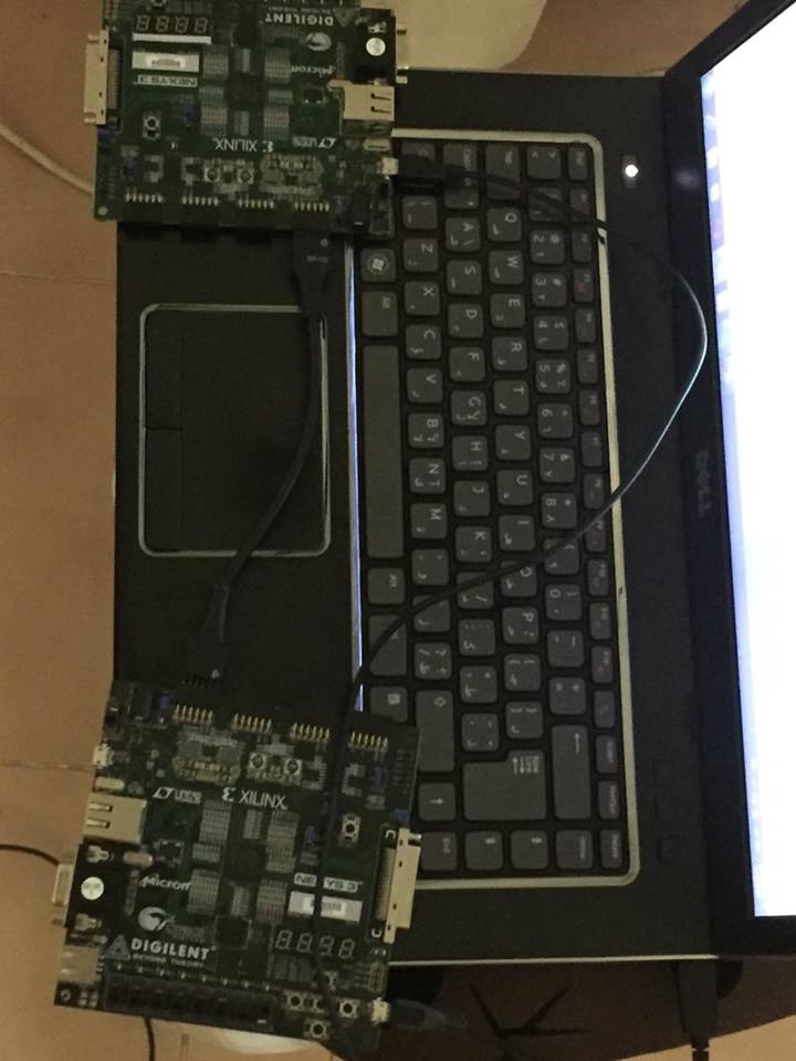
the project is to send world "like hello" from hyperterminl using uart
cable hello to spi master .. the spi master receive and send it by pmod
connector to spi slave.. the spi slave receive and send it back to pc
using uart cable..
Please enlighten me on how it seems that your in school to learn about
FPGA's and or vhdl/verilog and expect to just jump right into a working
example to solve what you should be learning and experimenting on. If
you need to understand spi and uart better, best suggestion is to get 2
arduino uno's, and a logic analyzer like the one found from
dangerousprototypes, find an easy spi example and have the 2 arduino's
transfer to eachother and serial print to monitor, have the analyzer
hooked up to watch the transactions between the 2 mcu's. you'll start to
see what is happening.
Anan H. wrote:
> i cant i need to finish this project in 15 days
First day: take some sheet of empty paper and a pen. Then sketch down a
design with it signal paths. Divide it into functional blocks and assign
it to hardware components.

Second and third day: find my HP and there all components you need.
Adapt it to your needs. Setup a test bench and proof the functionality
of your code.

Fourth and fifth day: implement the whole thing and get it running on
hardware.

Sixth to fifteenth day: go to the beach and have some fun.

But most important: start on the first day with a sober datapath
concept.
Please log in before posting. Registration is free and takes only a minute.
Existing account
Do you have a Google/GoogleMail account? No registration required!
Log in with Google account
Log in with Google account
No account? Register here.