I've known about the existence of copper pours for some time, but I
suppose didn't think I needed one, and up until now, probably didn't.

A little background: I have a little home project that uses a 50MHz quad
flat pack microcontroller with integrated 10/100 Ethernet MAC/PHY, which
connects to a RJ45 jack with integrated magnetics.  So there's a minimal
amount of external components required for my Ethernet interface.  Also
on the board is an I2S audio DAC going to a standard pair of RCA line
out jacks, and a simple linear power supply.  I designed a double sided
PCB with little regard to EMC, and it works, but when the Ethernet cable
is plugged in, the nearby TV shows interference.  (Which I find somewhat
amazing considering the TV is not getting signal from an antenna, but
from CATV).

So, after a little Googling I see what I essentially need to do with the
Ethernet traces/components, and it involves copper pour along with
keeping some traces near each other.  But my question is: is there a
reason to not apply copper pour to the entire board?  My current train
of thought is to copper pour both sides and connect it to ground.  But
is there much advantage to doing this?  I'll have to use copper pour
between the micro and Magjack, but is it worthwhile to use everywhere?

I know this is probably a very subjective question, with lots of
variables.  I'm looking for any input anyone has.  For the record, the
audio quality the current design is generating is fine.  It's just that
the Ethernet I/F is generating interference.
Jerry Milner wrote:
> (Which I find somewhat
> amazing considering the TV is not getting signal from an antenna, but
> from CATV).
I'm pretty sure your cable box and the ethernet switch or pc you connect
your board to share a protective ground wire.
Since there's no galvanic connection between the ethernet signal traces
and the nearby ground wire, it's the perfect setup to induce those emi.

> So, after a little Googling I see what I essentially need to do with the
> Ethernet traces/components, and it involves copper pour along with
> keeping some traces near each other.  But my question is: is there a
It's not quite that simple. It's the traces' impedance that's been
giving you a hard time. Since the impedance doesn't meet the IC-internal
pin-drivers' specification, there's some reflection happening and
therefore emission of rf-waves or exceeded voltage ratings on the line
occur.
Ethernet expects 100 Ohm line-impedance iirc. Impedance of your signal
traces is controlled by their geometry in terms of width and thickness,
distance to each other and distance to the next ground copper plane
(beneath).
Here's a tool to do the neccessary calculations:
http://www.mantaro.com/resources/impedance_calculator.htm#differential_microstrip2_impedance

> reason to not apply copper pour to the entire board?  My current train
> of thought is to copper pour both sides and connect it to ground.  But
> is there much advantage to doing this?  I'll have to use copper pour
> between the micro and Magjack, but is it worthwhile to use everywhere?
Not exactly between those two components but under the traces
interconnecting them.
Well there's no harm done using copper planes in almost-DC areas. If
anything, it adds to emc in terms of shielding/blocking emi from outside
your board and even from neighbouring traces on your board (crosstalk).
Plus, you don't have to spread out miles of ground traces =)

Regards,
Michael
I used your link to calculate the trace requirements for 100 ohm (it is
100 ohm for Ethernet).  I'm using standard 62mil FR4, 1oz, double sided.
I'd have to have 40mil wide traces separated by 10mil.  Can that be
correct?  All the examples and layout guidelines I've found online, in
addition to two TI eval boards use traces that are much thinner.  I've
seen conflicting information, so I'm very confused.  One source (SMSC I
believe) said to place ground traces or a plane near the differential
traces on the same side.  But the prevailing practice seems to be to put
a ground plane on another layer.

I guess my goal is not necessarily to eliminate the EMI if it will be
difficult to do so, but to make "easy" improvements to my next board
revision.  The main changes I want to make are schematic based, so I
figured I'd change some things while I'm at it that might help EMI.

Based on what I know now, and knowing this will be a 2 layer and not 4
layer board, and knowing that my current design functions, I'm thinking
of putting a ground copper pour on the opposite side of the Ethernet
traces and microcontroller footprint.  Beyond that, I'm not sure.
Yes, it can! The thinner the traces, the thinner the layerdistance to
the next ground plane. If the demo board have a 4+ layer board then the
next gnd plane is not 1,5mm away like it is in your case, its much
closer, like 0,2mm for example. This is the reason, why the traces and
clearance between it is smaller on this boards. If you have short
distances (about 1" length) there is simply no need to make this lines
impedance controlled, because there are much big disturbances of the
impedance in a short area that are based on the soldering pads and the
through hole vias. Can you post an image of the area of both sides
together? When you do this, we can help you much better.

I think there can be another reason for your problem, it could be that
the phy itself makes the emi not the traces to the rj45 but it's
essential to see your actual solution.
Attached files:
-

layout.png
6.4 KB
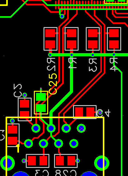
Hi, here's the part of the layout in question.  Red is the bottom layer,
green is the top.  The red pads along the top is the microcontroller.
The heavy green trace connecting to R1 - R4 is a Vcc feed.  The ethernet
jack is mounted to the top side (green).  The two pairs of red traces
parallel to each other is the ethernet differential pairs.  C25 and C28
are 0.1uF decoupling caps.  The capacitor footprints connected to
differential pairs on jack are 10pF required for ethernet PHY.  The
other two capacitor footprints connected to jack on Vcc pads are 0.1uF.

For reference, the distance between micro pads and nearest ethernet jack
side is about 700 mils.

And most importantly, but not obvious, is that there's a copper pour on
the green layer connected to ground.
Are you shure, these Capacitors and Resistors are needed? I have some
doubt about it! When its needed then you should make another routing:
first the capacitor and then the load. The resistors have to be within
the trace, so the "stubs" are as short as possible. In this case I think
it's no need for an impedance controlled routing but you should take
care about the trace length! The trace length should be as close as
possible to each other. If there is an edge you should compensate it as
close as possible to the edge. Another Problem is your VCC strip over
the differential pairs: this is a very big Problem! You should try to
make shure there is no disturbance of the groundplane in the area of the
differential pairs.
What I want to see is your VCC- and GND routing at the controller. Do
you have a Capacitor at (nearly) each VCC pin? GND connections as short
as possible to the next plane?
Jerry Milner wrote:
> Hi, here's the part of the layout in question.  Red is the bottom layer,
That's basically a pretty good layout already. I've seen worse in
commercial products ^^
Still, a few things crossed my mind:
- Use wider tracks for the signal lines as they have reduced
inductivity. Especially from those barey visible tracks from the
matching components to ground/Vcc.
- Avoid stubs (those "additional" tracks from the very signal track to
components), as they introduce additional reflection. This applies to R1
to R4, C1, C2, C4.
- Instead, directly place the pads of the components on the signal
tracks.
- Place an additional 100n capacitor to the common Vcc feed line for
R1-R4.

And yes, key to a EMI optimized design is an impedance-controlled
routing.
Christian B. wrote:
> Are you shure, these Capacitors and Resistors are needed? I have some
> doubt about it! When its needed then you should make another routing:
I do think so, since they provide proper termination at the "local" side
of the magnetic coupler.

> first the capacitor and then the load. The resistors have to be within
> the trace, so the "stubs" are as short as possible. In this case I think
> it's no need for an impedance controlled routing but you should take
Still, it's 100MHz signal with square pulses...
100% impedance match sure isn't required, but at this point the design
is still away from being anything close to best matched possible.
> care about the trace length! The trace length should be as close as
> possible to each other. If there is an edge you should compensate it as
> close as possible to the edge. Another Problem is your VCC strip over
> the differential pairs: this is a very big Problem! You should try to
> make shure there is no disturbance of the groundplane in the area of the
> differential pairs.
full ack.
Christian B. wrote:
> Are you shure, these Capacitors and Resistors are needed? I have some
> doubt about it! When its needed then you should make another routing:
> first the capacitor and then the load. The resistors have to be within
> the trace, so the "stubs" are as short as possible. In this case I think
> it's no need for an impedance controlled routing but you should take
> care about the trace length! The trace length should be as close as
> possible to each other. If there is an edge you should compensate it as
> close as possible to the edge. Another Problem is your VCC strip over
> the differential pairs: this is a very big Problem! You should try to
> make shure there is no disturbance of the groundplane in the area of the
> differential pairs.

Yes, the caps and resistors are required according to the micro
datasheet.  The other two caps from Vcc to ground are decoupling and
also shown in datasheet, although I think there could be a third one
added according to it.

Ok point taken, I'll put the resistors in the traces to eliminate the
stub.  As for the location of the 4 resistors and 4 caps on the
differential lines, some Ethernet layout guidelines recommend them to be
arranged in the way I have it.  And some Ethernet PHYs have the
resistors integrated into the die.  So as of now I think the order is
correct.

You are correct, the Vcc over the diff. pairs is bad.  I just didn't
have much motivation to correct it, but now I think I'm going to try and
reroute.


> What I want to see is your VCC- and GND routing at the controller. Do
> you have a Capacitor at (nearly) each VCC pin? GND connections as short
> as possible to the next plane?

I can certainly post more of the layout.  I might as well post the
entire thing.  Coming up soon in another post.
Michael H. wrote:
> Jerry Milner wrote:
>> Hi, here's the part of the layout in question.  Red is the bottom layer,
> That's basically a pretty good layout already. I've seen worse in
> commercial products ^^
> Still, a few things crossed my mind:
> - Use wider tracks for the signal lines as they have reduced
> inductivity. Especially from those barey visible tracks from the
> matching components to ground/Vcc.

Some confusion here, because the examples I've seen from silicon
suppliers use very thin lines for the diff pairs.  Then again, maybe
those are 4 layer boards.


> - Avoid stubs (those "additional" tracks from the very signal track to
> components), as they introduce additional reflection. This applies to R1
> to R4, C1, C2, C4.
> - Instead, directly place the pads of the components on the signal
> tracks.

Agreed.  Will modify.

> - Place an additional 100n capacitor to the common Vcc feed line for
> R1-R4.
>

Was thinking about doing that.

> And yes, key to a EMI optimized design is an impedance-controlled
> routing.
Michael H. wrote:

> Still, it's 100MHz signal with square pulses...
> 100% impedance match sure isn't required, but at this point the design
> is still away from being anything close to best matched possible.

I agree to you but when you see how short the distance is between the
phy and the rj45 I think it's not that problam when the differential
pairs are not routed with exactly 100 Ohm. If the diff. pairs are taken
over a longer distance I am the same opinion and there is no way out of
using the correct impedance.
Attached files:
-

layout1.png
11 KB -

layout2.png
25 KB
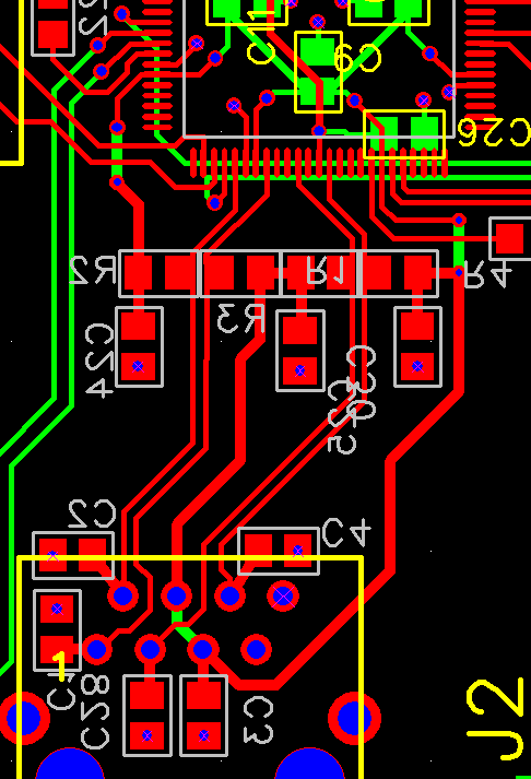
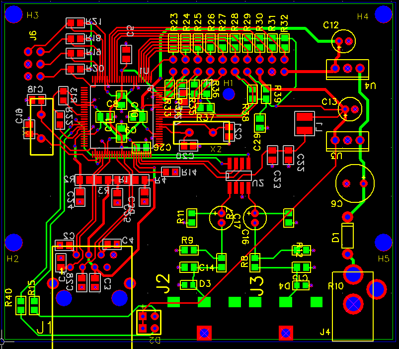
I made some changes, although I still would need to do some cleanup
before saying it's ready to go, like moving silkscreen text around :)

-Vcc is no longer under diff tracks
-capacitors at R1-R4 Vcc nodes
-vias to ground pour right on capacitor pads (no trace).  Need to change
the rest of components to this
-thicker traces in some places
-R1- R4 pads placed onto diff traces
-traces to caps/resistors made shorter where possible

I've attached both the Ethernet section in larger size, and the full
board not as large so you have an idea of the general layout.  The four
green footprints inside the micro are decoupling caps on the opposite
side of the micro.  The micro is a TI LM3S9B92 if you're curious, the 8
pin SOIC is a CS4335 audio DAC communicating via I2S (~1.5Mhz), the
20pin header near the top is for an LCD adapter board, and the 6 pin
header in upper left is JTAG programming.

My guess is the Ethernet section is by far the most critical.  The
serial audio tracks is probably not so much.  I'm guessing I have the
power pins on the micro fairly well taken care of.
ok, I'm back again :)
As I see the layout is much better than before, when you make a view of
GND vias near the pins and tht's (one at the start and the end) of the
differential pairs it could be a litte better (its needed because the
equalizing current should have only a short distance (as short as
possible) to meet the signals, its not so easy to explain why it's
usefull. I think another little thing you can do is making some trenches
into the GND plane near the audio area. the trenches should start under
the audio- chip and end at the board outline. So there is no influence
from the audio to the digital area.

Now the layout should be much more better and the emi problem schould be
past. A little better is the routing with the correct impedance but it's
only 100MHz and a short distance, so I think its not a big problem if
the differential pairs don't have the 100 Ohm.
Attached files:
-

layout2.png
25 KB
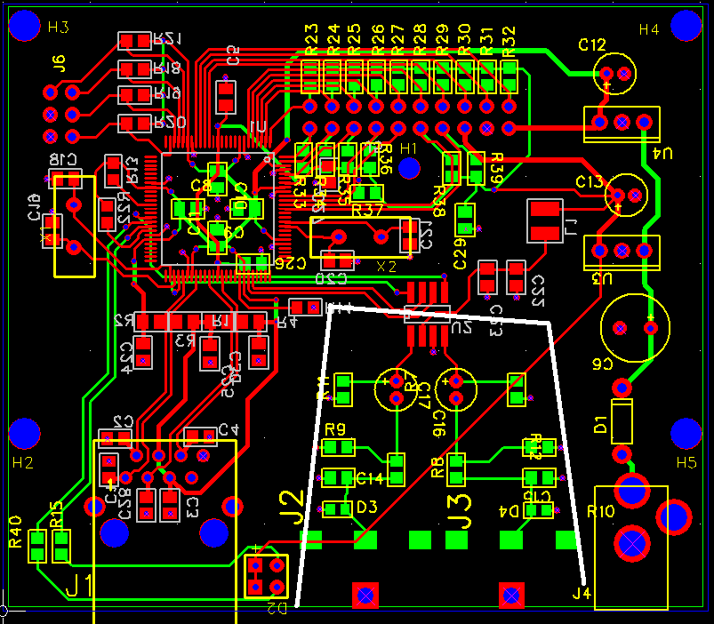
Christian B. wrote:
> ok, I'm back again :)
> As I see the layout is much better than before, when you make a view of
> GND vias near the pins and tht's (one at the start and the end) of the
> differential pairs it could be a litte better (its needed because the
> equalizing current should have only a short distance (as short as
> possible) to meet the signals, its not so easy to explain why it's
> usefull.

I'm not sure what you mean here.  Are you saying the ground vias near
the differential traces are bad?


I think another little thing you can do is making some trenches
> into the GND plane near the audio area. the trenches should start under
> the audio- chip and end at the board outline. So there is no influence
> from the audio to the digital area.
>

I have thought about splitting the ground plane.  So, I think you're
saying to put a trench around the entire audio area, with the digital
side of the DAC on one side, and the analog side of the DAC in the audio
area.

Would it be smart to not go all the way to the edge near the power
connector, as shown in the attached image (the white line), or should I
use a different method to attach the audio ground plane to ground?


> Now the layout should be much more better and the emi problem schould be
> past. A little better is the routing with the correct impedance but it's
> only 100MHz and a short distance, so I think its not a big problem if
> the differential pairs don't have the 100 Ohm.


This is great.  At least I know this board should perform better than
the current design.
Jerry Milner wrote:

> I'm not sure what you mean here.  Are you saying the ground vias near
> the differential traces are bad?

No, what I mean is, that it could be good, if you make some additional
GND vias near the pins of the phy and of the RJ45 witch are the start- /
endpoint of the differential pairs. At the phy side 1 via behind the 2
differential pair pins (in the middle of the 2 pins) and on the rj45
side 1 via behind the last pin of the differential pair. so you have 2
vias each pair to place.

the GND plane:

you should make a connection to the rest of the GND plane. these
connection can be a high value resistor (about 1 M Ohm or more) and a
capacitor (for example 1 µF 50V) (this is the best way) or another way
is to make a connection through the trench underneeth the I²C IC. The
reason is, that its usefull to have only one point where analog and
digital Gnd meets together.
Ok, so put a ground via between and at each end of each diff. pair, and
connect it to a ground pin on the PHY or RJ45, depending on which end
the via is located.  It does make sense in order to keep things
balanced, although I would have never thought of that.

For the ground pour (I haven't been calling it a "plane" because it's
only a double sided board), allowing the two ground areas to touch under
the audio DAC makes sense.  But wouldn't connecting it with a RC network
cause problems because there won't be a solid ground for the DAC?  Also
for that method, do you mean a cap and resistor in parallel?
thats exactly what I mean! The resistor is needed to have the same
potential in the 2 areas and the capacitor is for eliminating ripple
spikes. (this works only correct if there is no current flow from
digital to analog GND because of the high resistance) But, in your case
it will be enough, when you make a point beneath the dac where the two
gnd poors meet together.
Please log in before posting. Registration is free and takes only a minute.
Existing account
Do you have a Google/GoogleMail account? No registration required!
Log in with Google account
Log in with Google account
No account? Register here.