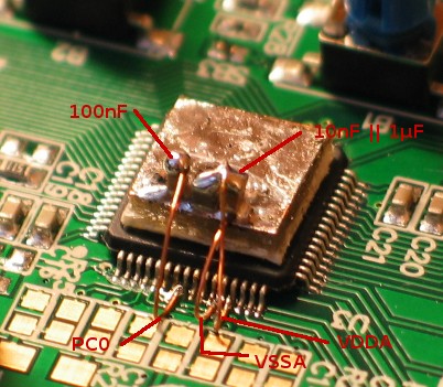
Lately, I decided to give the STM32F0 discovery board [3] a try. The ADC
seemed to be extremely noisy and I decided to investigate the problem.

I'd like to present my results here, just in case someone else
experiences the same problems.

Test setup:
  * STM32F0 discovery board
  * ADC clock from internal 14MHz oscillator
  * Analog input 10 (GPIOC0, configured as analog I/O, of course): I use
1.5 ADC clock cycles sampling time with this input
  * Internal voltage reference: I use the advised 239.5 ADC clock cycles
sampling time here.
  * FTDI USB<->RS232 converter
  * STM32F0 running at 48MHz PLL source, clocked from internal 8MHz RC
oscillator.
  * STM32F0 connected to FTDI via USART1, 19200 baud (highest setting
that works reliably with the internal RC oscillator)

I measured the internal voltage reference and an external voltage
applied to GPIOC0. For the voltage reference, I transmitted the raw ADC
values to the PC, for the external voltage I transmitted the calculated
millivolt-value.

Every value was converted to decimal (for easy debugging) and output to
the serial port. This should result in about 400 readings per second (I
didn't verify this, because that's not very important here).

The external voltage is generated by a 22k potentiometer connected to
VDD and GND. The cable from the potentiometer to the I/O-Pin is about
40cm long.

As a side note: The DC resistance of the potentiometer is far higher
than the suggested value which may have caused an unneglectable loading
of the potentiometer voltage divider and thus cause a voltage deviation
from the unloaded value. I'm aware of this but in this series of
measurements I was not interested in such effects (which may even grow
with the sample rate (higher sample rate -> more S&H cycles per second
-> more input current)). I take the ADC input voltage (which, for
absolute accuracy checks I measured directly at the ADC input) as given
and I am only interested in how to get low noise and a stable rading for
stationary signals.

At least 40e3 values were acquired for each dataset.


First test
----------
Potentiometer connected to GPIOC0. In the middle of the cable,
approximately 20cm from the PC0 pin header of the discovery board, I
connected a 100nF ceramic capacitor from PC0 to ground. The purpose is
to lower the dynamic impedance of the potentiometer. This reduces the
noise introduced by the ADC sample and hold considerably. Otherwise the
impedance of the potentiometer would be far too high.
The result was a disaster. You can see a plot of the acquired values in
PC0.pdf, dataset (a). The plot shows a time-series of the first 5e3
datapoints in the left subplot and a histogram of all datapoints in the
right one. Yes, the input voltage was only about 200mV in this case but
the noise wasn't better with higher values. The measured voltage
scattered roughly 100mV in total, a completely unacceptable result.

Second test
-----------
This time I selected the internal voltage reference as input. This
should rule out any problems caused by long external cables and bad
external setup. The result is plotted in vref.pdf, dataset (a).
At least the individual ADC counts are visible in the time series plot,
but the scatter is horrible, again. The center part of the histogram
looks somewhat "gaussian" but not the tails left and right. Something's
obviously wrong here.

As it turns out, ST didn't respect their own power supply decoupling
requirements. The STM32F0 discovery board doesn't seem to have any
capacitors on the VSSA and VDDA analog supply pins, whereas the
datasheet tells us 1uF || 10nF is required [2].
I put a piece of PCB onto the top of the MCU with double sided adhesive
tape and soldered the decoupling capacitors onto it (see setup.jpg).

Third test
----------
I repeated the second test, now with the decoupling capacitors in place.
The result can be seen in vref.pdf, dataset (b). The result looks much
better, the tails in the histogram have gone, the scatter is smaller.

This was a first step, but the results of the external voltage didn't
improve. I decided to move the 100nF cap very close to the I/O pin and
therefore placed it on top of the MCU, too (see setup.jpg).

Fourth test
-----------
Repetition of the first test. Result in PC0.pdf, dataset (b). Almost all
of the scatter is gone. Don't worry about the different average value.
I've touched the potentiometer between the tests. Please notice that the
highest bar of the histogram goes up far higher but I set a limit of 0.3
on the y-axis.

Summary, possible explanations and lessons learned
--------------------------------------------------
Apart from the proper supply decoupling, it is extremely important to
drive the ADC input with a very low impedance. This seems obvious -- the
datasheet ([2], Electrical characteristics, Table of R_AIN,max for f_ADC
= 14MHz) lists a required maximum impedance of 400 Ohms for the fastest
sampling time -- but you have to keep in mind, that the impedance must
be provided directly at the MCU pin. The 20cm wire to the capacitor in
the first test completely messed the results up.
For slowly varying inputs (like a potentiometer) it may be sufficient to
connect a capacitor directly to the analog input like I did. (Please
note that I didn't try out the minimum size of this cap, but the 100nF
seem reasonable as you can see by this eyeball-calculation: The S&H
capacitance is about Cint = 8pF, according to the documentation [2]. The
ADC has 12bits, thus we have 4096 values. If we allow a voltage change
of the external capacitor Cext of one step size during the sampling
process and assume that all current is drawn solely from Cext, we arrive
at the conclusion that Cext > Cint*4096 = approx. 33nF. Add some safety
margin and you arrive at 100nF for a standard value.)
If you want to digitize a fast changing signal, you'll probably need a
very fast buffer close to the ADC input; The fastest sampling time is
only 110ns(!) and the buffer should keep the ADC input voltage stable
during this time.

References
----------
[1]: RM0091: Reference Manual, STM32F05xxx/06xxx advanced ARM-based
32-bit MCUs
(http://www.st.com/web/en/resource/technical/document/reference_manual/DM00031936.pdf)
[2] STM32F051x4 STM32F051x6 STM32F051x8: Data sheet
(http://www.st.com/web/en/resource/technical/document/datasheet/DM00039193.pdf)
[3] UM1525: User Manual, STM32F0DISCOVERY, Discovery kit for STM32 F0
microcontrollers
 (http://www.st.com/st-web-ui/static/active/en/resource/technical/document/user_manual/DM00050135.pdf)
Attached files:
-

setup.jpg
70 KB
Many thanks for providing your results!!

I'm not using an STM32 controller but I do believe, your conclusions
apply to other controllers, like LPC, too.

Although I repeatedly failed getting precise readings of the ADC on a
LPC175x I did never perform such a systematic analysis.

I was using an INA193 current sensor IC connected to the ADC input.
Unfortunately, most opamps don't like capacitors at their outputs and I
doubt the outputs are of low impedance on the time scale of the ADC's
sampling. So I would end up with a RC connected from the opamp output to
the ADC input.
To be a bit more precise: It is the sampling process of the sample and
hold stage which may cause this troubles. They are therefore not
restricted to the STM32 series ADC. You can run into these problems even
with external ADCs.

I learned this after posting my results. If had known this before, I
would have chosen a different title, I think.

You are right, capacitive loads lead to problems with most opamps. The
typical solution seems to be an opamp followed by an RC lowpass, as you
propose.

There is some freely accessible literature on this topic which deals
with the "correct" design of the component values. Just search for "sar
adc driver" and such and/or have a look at [1,2] for a first start.


[1]:
http://www.edn.com/design/analog/4325145/2/Start-with-the-right-op-amp-when-driving-SAR-ADCs
[2]: http://www.ti.com/lit/ml/slyp166/slyp166.pdf
Please log in before posting. Registration is free and takes only a minute.
Existing account
Do you have a Google/GoogleMail account? No registration required!
Log in with Google account
Log in with Google account
No account? Register here.