Hi,

i am new to analog design, and in need of some feedback.

I need to interface an analog signal with max swing 1V to 4.9V (@400Hz)
to a ADC powered for 0v to 3.3V.
After a lot of reading i have a circuit that simulates nicely.

I use 3 RRIO op-amps.
- first opamp does the required attenuation and offset according to the
transfer function that i calculated (Vout = 0.846 * Vin - 0.846)
- second opamp is an active unity gain LP anti-alias filter (@ 1KHz)
- third op-amp is a unity gain buffer to drive the SAR ADC.

I am happy with the simulations but because this is my first design, am
not sure if I am missing something in the signal chain.

the output to the ADC has a max swing 45mV to 3.18V. close enough to the
required 0V to 3.3V. (right?)

Any thoughts?
I do have to measure signals with offset as well, but I do not
attenuate.

If you have the possibility set different ref voltages to your ADC, then
you can start measuring at 1 V.

To not touch 0V in your design seems critical for me, because that
already is an inherent error, or do you calculate at the end?

In general I suggest the less OpAmps the less noise you get on your ADc
signal, which is always better.

second opamp is an active unity gain LP anti-alias filter (@ 1KHz)


technical talk? what exactly is the difference between the 2nd and 3rd
opamp? active unity gain and no active unity gain, for me it would be
exactly the same since opamps are always active elements...
Attached files:
-

design.jpg
200 KB
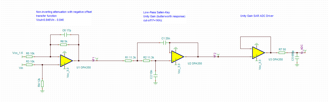
Hi thanks for the response.

The ref voltage of the ADC is the Supply voltage, so i need attenuation.

The opamps are powered from the same supply (0v to 3.3V). The one i
chose OPA350, will do RRO within 10mV (my 45mV isnt the best i guess).
So, how can someone reach true 0V on the output?

as for the active terminology, am probably not stating right.
I found notes on how to drive SAR ADC's. They propose a unity gain
buffer followed by an RC filter for charging the input capacitor of the
ADC. that is the 3rd opamp+RC.
The second is the active LP filter.

i like the idea of less devices less noise. Could I get rid of the third
one and have the RC filter at the output of my 2nd one?

i am attaching the circuit for ease.
the last buffer always is a good idea, as you said because the cap of
the s&h of the ADC need sufficient current.

I would power my OpAmps with dual supply, thats the only way to reach
reliable 0V. But of course it always depends on accuracy and do on, if
its worth to put in another power supply, that sup to you to design or
choose from.

I never used an active low pass, so I dont know if that really is a
benefit.

I just use passive ones, for me that worked fine, but there are of
course negative sides to that as well, since an passive low pass will
kind of draw current frmo your signal and so on.

If you never have built up something like this I would suggest you start
as simple as possible and work your way up, since that is how all
Appnotes and papers did start as well, you can get complicated as much
as you want, after you got 1 design to work, and usually the simpler the
more likely to work.

for example, where will you get your resistors 6,2k from? not even
speaking of the 17pF in your first feedback path :)

So start with basic E24 values, do a simple design that works , then
start doing better and so on..
the design will be on a prototype pcb

- the 6K2 resistor is
http://uk.farnell.com/panasonic-electronic-components/era2aeb622x/resistor-metal-film-6-2kohm-0/dp/2324793.

and
http://uk.farnell.com/avx/04025a180jat2a/cap-mlcc-c0g-np0-18pf-50v-0402/dp/1740572
for the cap.

i will use the OPA4350 (quad version of the OPA350). leaves me with one
extra opamp spare (if needed later on)

Thanks sdf for the nice discussion.
np,

one more hint for your 0402 choice :)

its of course a lot harder to handle than 0603, still doable I think,
but the pads get physically closer, so the parasitic capacitance I would
say is about 1 pF already, that shouldnt do anything in your design, but
in general should be on your mind when building more critical circuits.
Please log in before posting. Registration is free and takes only a minute.
Existing account
Do you have a Google/GoogleMail account? No registration required!
Log in with Google account
Log in with Google account
No account? Register here.