Hello everbody,

I am in a very big project with an ALTERA FGPA Cyclone IV. This FPGA is
going to control several systems and every  system has its own
configuration file sent by SPI protocol  which it is already implemented
like a VHDL module in the FPGA. In the start up of the system, the FPGA
is sending the intial configuration file for a default hardware which is
the most commun. This configuration file is stored in a FIFO memory with
the possibility to be modified "on fly" thanks to the "IN SYSTEM MEMORY
CONTER EDITOR" tool provided by Quartus II SW. So if the Hardware
changed we can use this tool to change the initial configuration SPI
file....

But we don't want to use this tool and we want to change the initial SPI
config file in the FIFO using the a command recevied by ethernet protcol
(The FPGA has also implemented a Ethernet module to communicate with a
PC). This command is going to be read by the FGPA and accordint to this
we will change the initial configuration file.

See below the instantation of the FIFO memory:


 i_SPI_INIT_RAM : entity WORK.SPI_INIT_RAM
    generic map (
      ADDR_SIZE => SPI_MEM_SIZE,
      DATA_SIZE => SPI_MEM_RDOUT'length,
      INIT_FILE => "../fit/SPI_INIT_RAM.mif",
      INST_NAME => "SPIF"
    )
    port map (
      clock    => CLK            ,
      wren      => '0',
      address => SPI_MEM_ADDR,
      data      => (others => '0'),
      q        => SPI_MEM_RDOUT
    );

As you can see there is a GENERIC ==> "INIT_FILE" where you have to
indicated the path of the file you want to load. And it is this path
what I want to modify "on fly" when I receive the ethernet command...

Any idea how to implement this?

Thanks.
What you’ve got here is a plain RAM, not a FIFO.

The INIT_FILE generic is evaluated during synthesis/assembly at design
compile time.
The purpose of this is that the memory in question is initialized after
FPGA configuration with what the initialization file described at
compile time.

By using the ‘In Memory Content Editor’ you are able to update the RAM
contents at runtime.

Obviously the configuration bitstream is not affected, meaning that when
you reconfigure the FPGA, the RAM will hold its original contents.

To update the RAM contents via Ethernet, all you have to do is to
provide a write port for the Ethernet module.
This is the same concept as how the ‘In Memory Content Editor’ is
updating the RAM behind the scenes.

It looks like the RAM is a generated IP, so you can add this port by
using the wizard.

Cheers, Roger
Hi!!! Thank zou vey much for your answer, Yes I can provde a write port
to the RAM memory but then I observe the next problem: When I  power
off/on the system, the RAM will load the init file indicated in the
generic. And what I would like to keep the last file loaded. Is there
any other possible solution for this?

Thanks
How is your FPGA being configured?
If it’s Active Serial trough an EPCS device, you could use an empty
sector as nonvolatile storage.

Cheers, Roger
Attached files:
-

Flash.jpg
260 KB
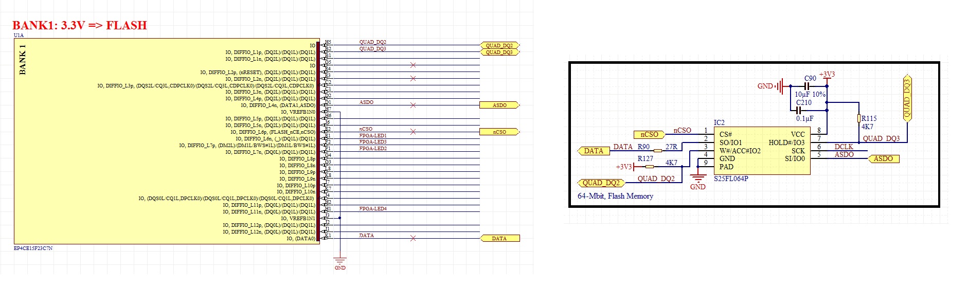
Hello Roger, Thanks again for your answer. See the picture attached to
take a look to the connection between the FPGA and the flash. I guess
that I can do what you are indicatind "use an empty sector as
non-volatile". But Could you explain in detail how to get this? Or How
can I search this in internet?

Thanks.
The Flash is accessible from user logic. So all you need is the S25FL064
datasheet and have a look at the instructions: READ, RDSR, WREN, SE, PP

You can read a configuration in one go with READ.
To update a configuration you’ll have to erase the sector (SE) and write
the data with one or more page program (PP)
All modifying instructions require a write enable (WREN) upfront.
Erase/program completion can be checked with read status register
(RDSR).

However, your circuit connects the Flash in Quad mode to the FPGA.
AFAIK none of the Altera stuff Is making use of this.
Which suggests that you might have something in your design that
Already connects to the Flash, especially since the Flash is quite big
compared to the bitstream size.
In that case you might want to team up with the solution in place.

Cheers, Roger
ok I will try it and I will tell you how it was....

Thank u very much!
But I don¨t know how to access to the flash from the FPGA? Can I do it
with the currento flash configuration?? Is there any Altera IP
Megawizard function to make everything easier??

thanks
Your Flash configuration is fine. There are two suitable IP for this:

-  EPCS Serial Flash Controller
-  Avalon Serial Peripheral Interface

Both of them are Avalon/Qsys IP and only take care of the SPI
serialization/deserialization part.
Formulating Flash commands, programming/erasing etc. is not abstracted
with this.
Altera provides a software driver for that but nothing in HDL.

Anyways, you can use almost any SPI IP or roll your own, this is super
simple stuff.
As for the Flash commands, I doubt that you’ll find something ready-made
that fits your needs.

Cheers, Roger
Please log in before posting. Registration is free and takes only a minute.
Existing account
Do you have a Google/GoogleMail account? No registration required!
Log in with Google account
Log in with Google account
No account? Register here.