Hi,

this topic is about the PCB for a wireless master in the OpenHR20
project.
A thread about the OpenHR20 firmware can be found at
http://embdev.net/topic/118781

A german article about OpenHR20 can be found at
http://www.mikrocontroller.net/articles/Heizungssteuerung_mit_Honeywell_HR20
(information might be a bit outdated).

Some schematic of a PCB can be found in the SVN repository at
http://openhr20.svn.sourceforge.net/viewvc/openhr20/rfmsrc/doc/master_board/

The 10-pin connector is the same as the one on HR20, so there is JTAG
and a RX/TX. For connection to a router as WRT or FritzBox, a
serial-to-USB converter might be necessary. But I'm not sure whether a
FTDI driver would work on a FritzBox.


Feel free to contribute if you are interested in designing or if you
already have a prototype and want to share your findings.

Regards
Marco
Ok, seems that the project Freetz [1], a custom firmware for FritzBoxes,
supports the FTDI serial converters [2].

Would it be better to integrate a FTDI converter on the master board, or
connect two boards using the 10-pin connector?

And is it ok to supply the master board from USB?


[1] http://trac.freetz.org/wiki/freetz (german)
[2] http://trac.freetz.org/wiki/libs/ftdi (german)
Attached files:
-

master_schematic.png
21 KB -

master_board.png
28 KB
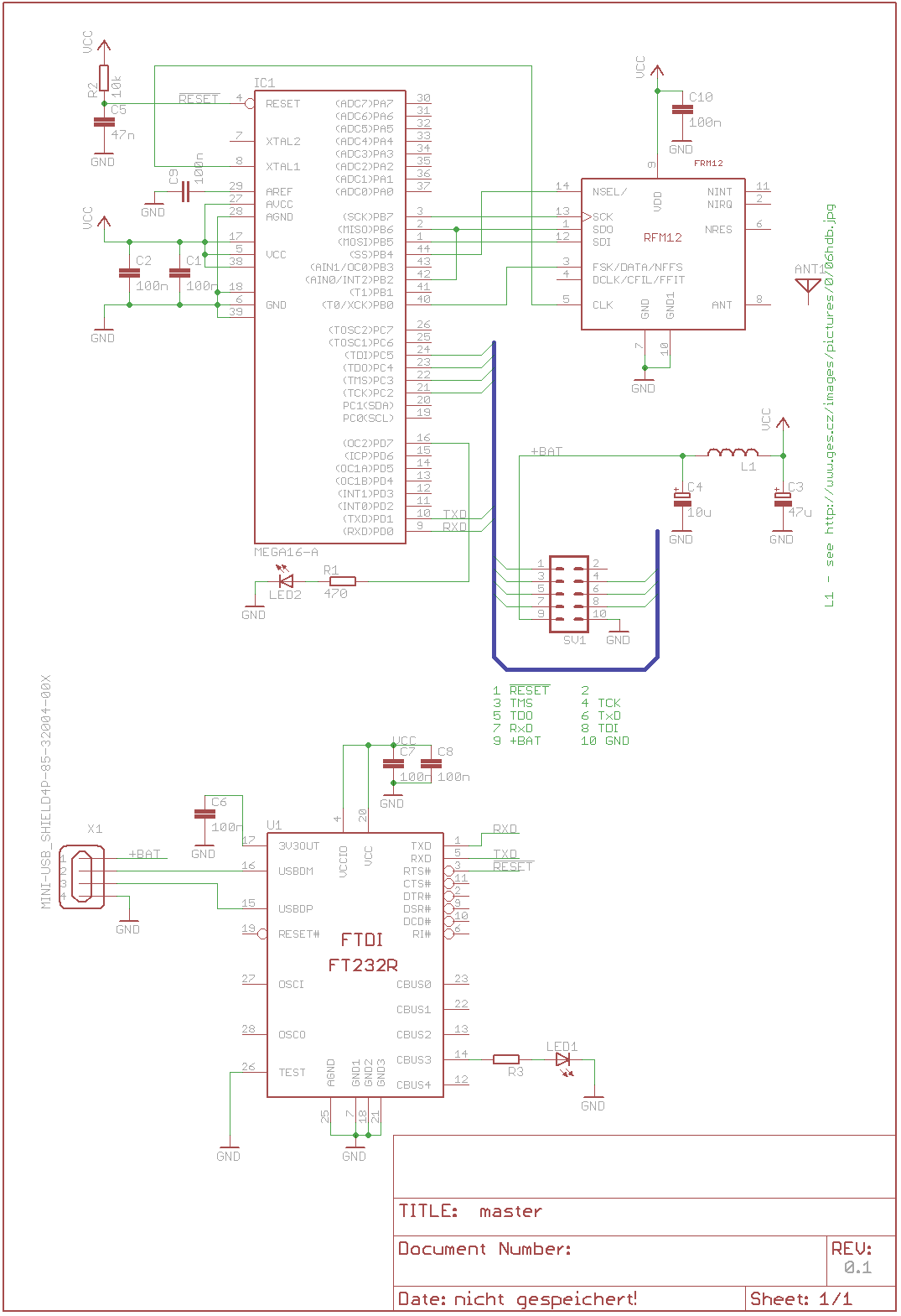
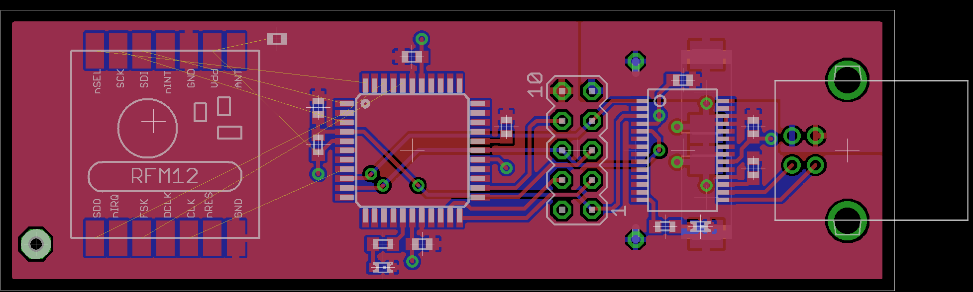
my first try (I obviously not completed routing yet ;)
Attached files:
-

master_schematic_v02.png
21 KB -

master_board_v02.png
32 KB
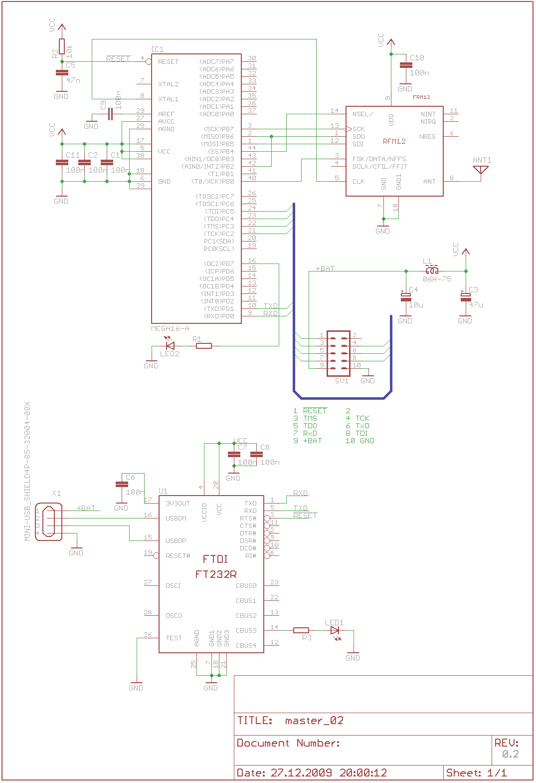
ok, next version :)

If it is connected directly to a serial interface, the FTDI USB
converter part can be cut.
All parts except the coil are mounted on the top, and even the coil
could be mounted on top if it is isolated a bit.

I've no idea what kind of antenna should be used on the RFM12 modules,
so feel free to contribute, also if you find some errors :)

br
Marco
Hi Stan,

Yes your board looks good. I have add ,at my master, a second led which
show the transmission of the sync packet. This looks usefull for
diagnostic purposes. Maybe it could usefull to connect some additional
portpins to pad for expansions.

bye

Ronny
Why not use a mini USB ? like
http://www.reichelt.de/?;ACTION=3;LA=444;GROUP=C126;GROUPID=3213;ARTICLE=52003;START=0;SORT=artnr;OFFSET=100;SID=28f4vsnawQARwAAEpdONg3c5eae9c8e6da654f04e58b63c91e9bb

Ronny
Attached files:
-

master_schematic_v03.png
22 KB -

master_board_v03.png
34 KB

Hi Ronny,

great idea! Are these four enough? Is it ok to use the INT-inputs? They
are located at a free corner ;)

br
Marco
Hi,

I can't see any problem with P1-P4 lines. We have many free lines
because this MCU is too big for this aplication. But it is smallest CPU
with JTAG debuging from Atmel.

- current SW need some communication buffers and use ATmega32 not
ATmega16. Pinout is same, difference is volume of RAM (and Flash)

- RTS# signal for RESET# can be problem if we want to use simple
terminal for debugging. Can you add jumper into this signal?

- Antena can be lambda/4 wire, for 868 it is 86mm (L[mm] =
75000/frequency [MHz])

- Antena can be path on PCB, due to PCB effect it must be 10-20% shorter
than wire. Wire is usualy better.

Happy new year! Jiri
For which purpose the FSK-pin is used? All functions are available via
SPI.
FSK pin is not used and in this case it need pull-up resistor. My
original design use pull-up inside MCU, it save soldering of one
component. Just a trick, nothing more.
Please remove R2+C5 components. ATmega contain better startup reset
circuits inside and it complicate external reset signal connection
(capacity load).
Thanks for your suggestions, I'll take care of them when I come back
from skiing :)
@Ronny Kunze: can you add your modification with second led into source
code? If it is not use incompatible pinout, sure.
If you need access to SVN tree, please send me email.
Attached files:
-

master_schematic_v04.png
22 KB -

master_board_v04.png
33 KB

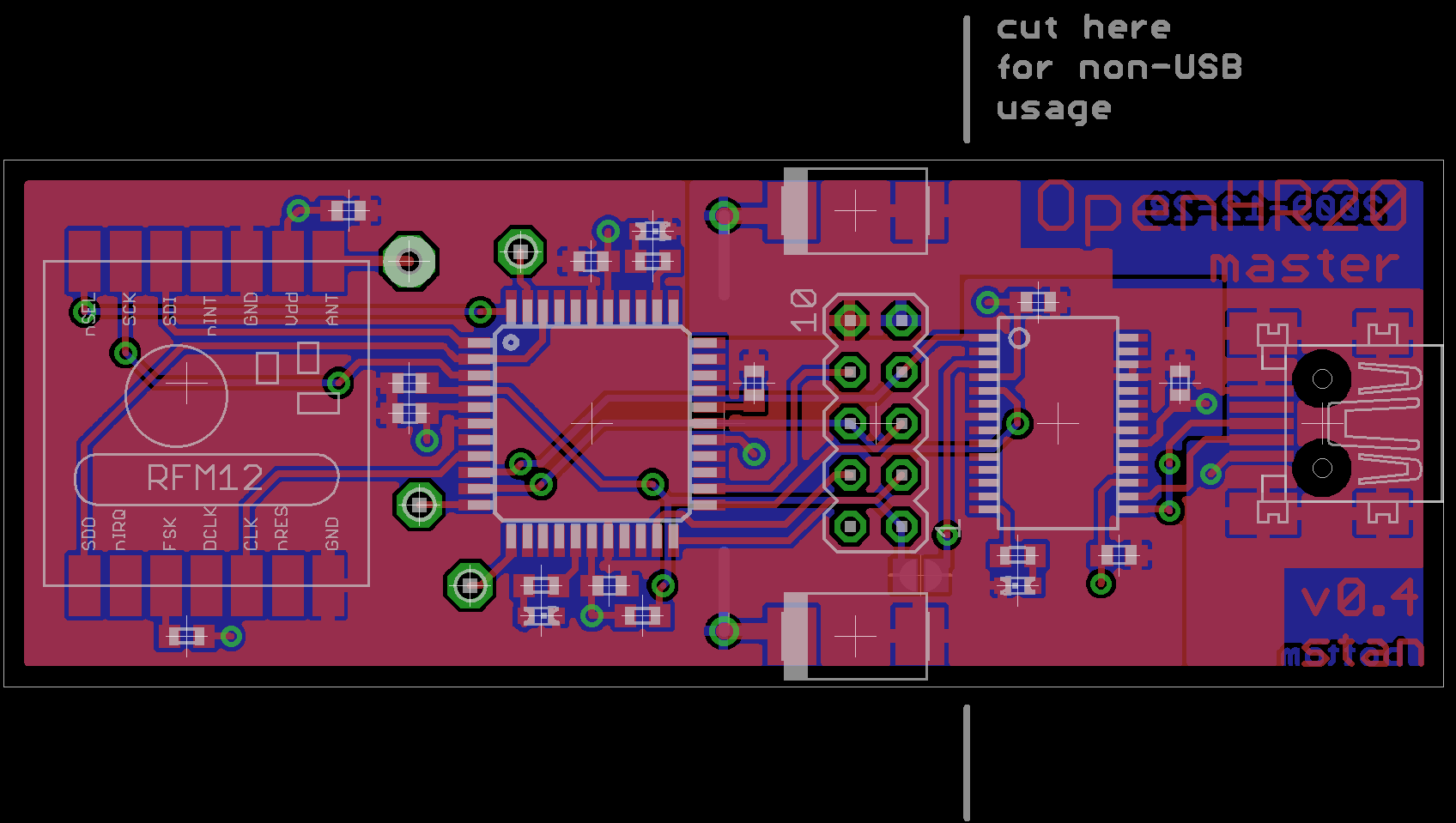
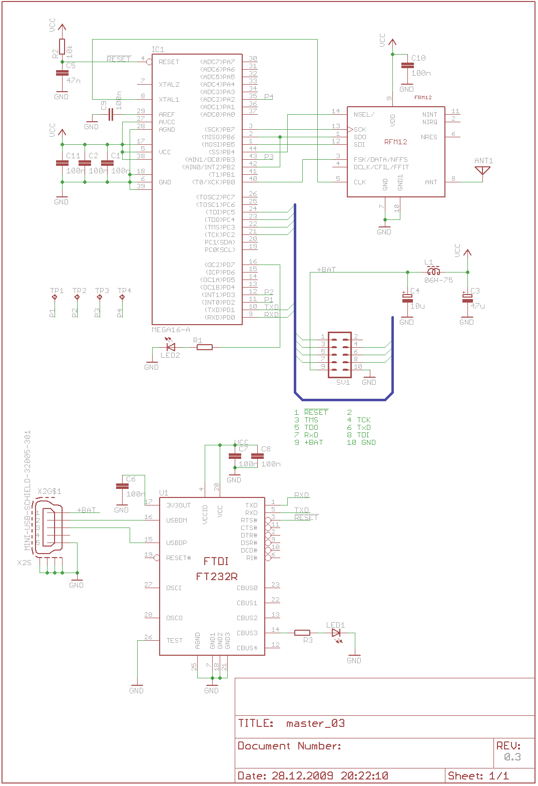
Hi,

here are the changes for version 0.4:

jdobry wrote:
> - current SW need some communication buffers and use ATmega32 not
> ATmega16. Pinout is same, difference is volume of RAM (and Flash)
Atmega16 changed to ATmega32.

> - RTS# signal for RESET# can be problem if we want to use simple
> terminal for debugging. Can you add jumper into this signal?
done

> - Antenna can be lambda/4 wire, for 868 it is 86mm (L[mm] =
> 75000/frequency [MHz])
> - Antenna can be path on PCB, due to PCB effect it must be 10-20% shorter
> than wire. Wire is usually better.
ok, I keep the the via to solder a wire.

> FSK pin is not used and in this case it need pull-up resistor. My
> original design use pull-up inside MCU, it save soldering of one
> component. Just a trick, nothing more.
external pull-up resistor added and connection to ATmega removed.

> Please remove R2+C5 components. ATmega contain better startup reset
> circuits inside and it complicate external reset signal connection
> (capacity load).
well, if they are not populated there's just 1 mm of extra wire on the
PCB.

Test point number four is replaced by an extra LED as suggested by
Ronny.

Any more suggestions?

BR
Marco
Attached files:
-

master_04_eagle3d_top.png
110 KB -

master_04_eagle3d_bot.png
57 KB
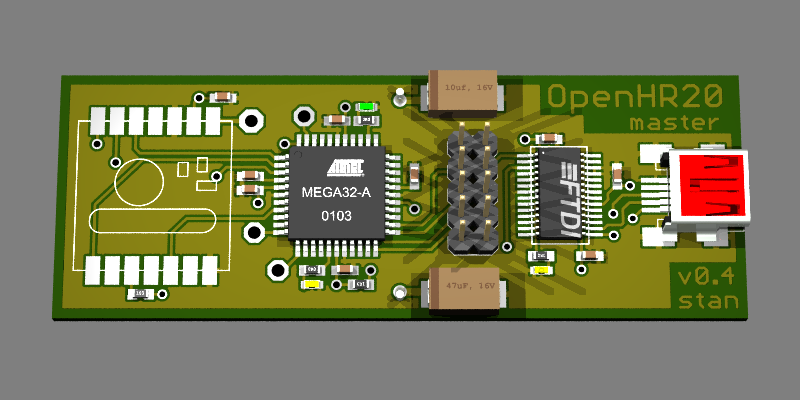
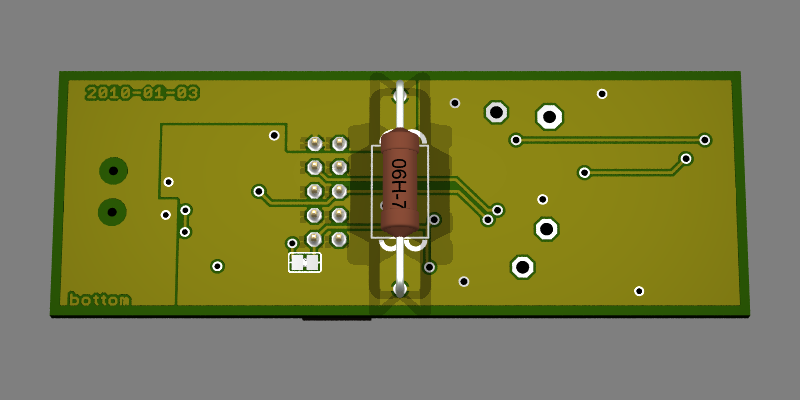
here's some kind of preview :)

Of course L1 (at the bottom) is not a resistor, but it is the most
similar package.


Another idea:
would it be better to rotate the RFM12 by 180° so that the antenna is
located at the left edge of the PCB? Or is it ok right now because a
vertical antenna can be used?
What do you think?
I can't found any problem with this PCB.
Rotation of RFM12 is not needed. But I have another idea to add ground
soldering point close to antena. It can be useful when somebody will
need connect antena via coaxial cable.

Jiri
Thanks Jiri :)

I'll add a point for soldering a GND connection and tomorrow I'll place
my order.
Hello People,

I will modify my code to work with your LED port and send a patch in the
evening.

Ronny
Marco G:

You can compare rendered image with real here:
http://openhr20.svn.sourceforge.net/viewvc/openhr20/rfmsrc/doc/master_board/master_without_ftdi.jpg?revision=274
Only one difference except missing FTDI is used inductor. I was use
10uH.

Could you send me source files for update documentation?
Today I plan to replace old prototype board with your PCB and in this
case source code will not fit into schematics in SVN. Thanks, Jiri
OPPS!

I found problem. This design can be used without FTDI with 3.3V power.
But with FTDI and USB power RFM12B will be overpowered.
Recomended power range for RFM12B is from 2.2V to 3.8V
5V from USB will not damage it (maximum is 6V) but it is outside range.

Jiri
Yes you're right, I intended to use a RFM12 (without 'B') on master
because of the 5 V USB supply.

AFAIK there's no difference between RFM12 and RFM12B, but I'm not sure.
here is differences between RFM12 and RFM12B:
http://news.jeelabs.org/2009/05/06/rfm12-vs-rfm12b-revisited/
Its easy to fix: remove L1 and use the 3.3V Ftdi Internal
Voltageregulator it drive up to 50mA - is that enough for the rfm12???
@Ralf H.:

50mA is enought

- RFM12B have 26mA maximum
- ATMEGA32 (5V/10MhZ) need 15mA maximum
- and remaining 19mA for LEDs

Problem is that you must crop VCC layer on back side, because FTDI must
be powered from 5V, remainnig part from 3V3

PS: I was also use RFM12B and I miss information that pull up on FSK is
not needed. It is not problem on this PCB, but I was can save soldering
of one wire and resistor inside valves.
Jiri Dobry wrote:
> Could you send me source files for update documentation?
> Today I plan to replace old prototype board with your PCB and in this
> case source code will not fit into schematics in SVN. Thanks, Jiri

I'll send them to you this evening :)
Ralf H. wrote:
> Its easy to fix: remove L1 and use the 3.3V Ftdi Internal
> Voltageregulator

It's not that easy:
VCCIO must be connected to 3V3OUT so that the UART pins are driven with
3.3 volt. Otherwise TX would still have 5 volt high level which would
cause problems with ATmega.
Attached files:
-

mod.JPG
110 KB

> VCCIO must be connected to 3V3OUT so that the UART pins are driven with
> 3.3 volt. Otherwise TX would still have 5 volt high level which would
> cause problems with ATmega.

I thing that it is easy, see to the pictures.

- 1 wire to crop.
- 2 new wires
- do not use inductor
Attached files:

Connection on bottom side for modification.
@ Marco

Hi  Marco,

are there master boards left ?
I am interested in one.


Ludger
sorry, I haven't got any left.

But I would fix the bug mentioned above and order some new ones. The bad
thing is that they need at least 2 weeks to arrive...
hello marco g.

i would also be interested in a masterboard (or two).
Can sell 2 to me / shipment to germany ?

regards reinis
Hello,

i have one board more then i need. but not the simular design. its a
little bit smaller. and some components are in 0402. I get these boards
next week.

Ralf
I've added my schematics to the repository, including a fixed version
0.6
FTDI TX/TX LED have wrong connection. This signal is inverted and open
collector.
That might be the reason why that LED never showed anything on my board.
Thanks for the finding!
Has anyone tested this circuit with the FTDI and powered from USB? I am
facing the problem that there seems to be no communication from the FTDI
to the ATMEGA or from the FTDI to the PC.
I can not receive or send anything from the PC.
I am running it for nearly 3 years now, powered from USB. With the
corrections shown above.
I have used the board and schematic 0.6 from the SVN without any
changes. Which settings are you using for the UART connection? I tried
38400 baud with 8n1 and do not receive a single Byte in my terminal
program.

Which Atmel do you exactly use on your hardware? The schematic says only
"Mega32-A" which is not really a correct part number. Maybe I have
ordered the wrong controller? But I was able to flash an debug the
software on the controller. Sadly I have no experience with Atmel
controllers and the AVR Studio..
Version 0.6 should be fine. 38400 baud and 8N1 is also fine.

I am using this one: ATMega32-16 AU
http://www.reichelt.de/Atmel-ATMega-AVRs/ATMEGA-32-16-TQ/3//index.html?ACTION=3&GROUPID=2959&ARTICLE=50553&SHOW=1&START=0&OFFSET=500&;

Does the FTDI enumerate correctly? Have you used the FTDI programmer
utility to change the EEPROM seetings to 500 mA?
Yes the FTDI is correctly recognized by the PC and I am able to connect
to the serial line with putty. I have changed the power setting in the
devices EEPROM now, but this made no change. I still do not receive
anything from the ATMEL controller.
I checked the voltage on the Atmega and there are correct 3.3V on the
device. Also I am able to debug the controller and there does not seem
to be any problem with the hardware.

I am using this controller:  ATMEGA32A-AU
Have you correct fuses in MCU? It use external 10Mhz clock from rfm12
module
I don't know.. I have found a fuses section in the code and checked the
controller fuses against these settings. Now I got these fuses:

FUSES =
{
    .low = 0xA0,
    .high = 0x91,
};

The RFM12 module is also soldered and has the correct voltage supply. I
do not hava a oscilloscope so I can not check the clock. But would it be
possible to debug without proper external clock?
Attached files:
-

UART-Problem.png
2.8 KB
Hi,
my problem with the master is still not solved. It seems that the UART
generated by the ATMega ist not with the correct speed.I have attached a
picdump from my logic analyser. As you can see the trransmit from the
controller to the FTDI is really slow. On the RXD line sou can see a
transmission from the  FTDI to the ATMega with 38400 baud.

Has anyone a clue why the controller sends so slow? I have checked the
clock from RFM module which is at the correct 10MHz.
Alright my problem is solved!
In the init routine for the UART I had to switch the setting of the
baudrate and the other settings. First the UART is set up properly and
then the baudrate is written into the registers. I don't know why but it
works now!

Well now comes the real work. How can I figure out if the master is
working properly? I have found several commands in the code like 'H' or
'Y' but there are few more. Is there any documentation about the
commands?

Is it correct that I have to set the time with the 'H' command first
before the master tries to send anything?
You need to run daemon.php in \repo\rfmsrc\frontend\tools to interact
with the master HW.

I used WAMP package for testing on my Windows machine.
Now is runs on my Fritzbox 7270v3.
How have you used this on windows? PHP is normally not able to access
the serial interface on windows.
You're right. I have used SerProxy and then connected to it like:
1 | $fp=fsockopen("127.0.0.1",5334);
|
http://www.lspace.nildram.co.uk/freeware.html
Okay, seems to work now - somehow..

Do I understand it correct, that the daemon.php is the interface to the
serial console. It takes command from the database and puts them on the
console? The frontend uses the same database to creat commands which are
then processed by the daemon?

When I use a terminal program to view the serial output of the master
then there are sometimes lines which begin with "ERR". Are these
received packets from unkown nodes?
All your observations are correct :)

I get about 5 times more ERR packets than regular packets (with 5
valves), so I think that is ok.
I have some master boards left. If anyone is interested, please let me
know.
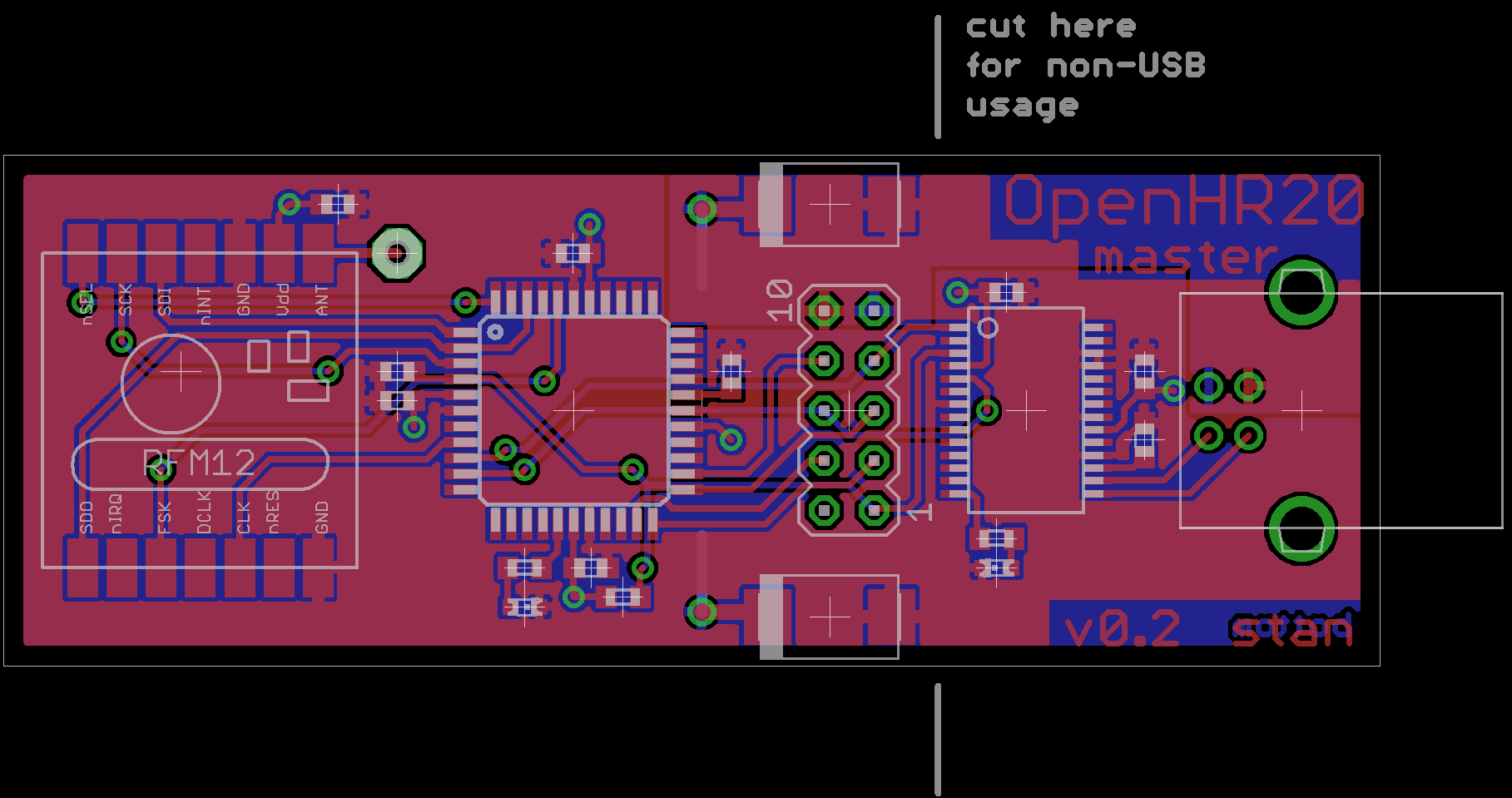
Hi,

I have changed the connection at the FTDI Communication LED and resized
the whole Board. Now it's not possible to cut it into two pieces, if you
would use it only with 3v3 uart. But I think thats not a problem - the
whole Board is now smaller then the "uart only" part in version 0.6.
Also I deleted the testpoints (TP1, TP2, TP3). I think the testing phase
is over and if anybody need an debug output, he can solder it direct to
the atmel.

In the attachment is the new layout - i think anybody could commit it to
the svn (or git [or both]).

Greets,
Michael
Tomek Z. wrote:
> I have some master boards left. If anyone is interested, please let me
> know.

Is there anybody else, who got a board left? Plz drop me a line.

Greetz
Martin
Hello,

I had ordered some master boards with my new layout... I think, you can
have one of them. But they are shipped from china an haven't arrived
till now.

If you want one, write me a message and i will notice you, if i have the
boards here.

Greets,
Michael
Hi,

I got version 6 boards from a friend and wonder if there is a reichelt
"basked" somewhere or a list of part numbers for reichelt / conrad in
germany.

Thanks
Ansi
Please log in before posting. Registration is free and takes only a minute.
Existing account
Do you have a Google/GoogleMail account? No registration required!
Log in with Google account
Log in with Google account
No account? Register here.