Hallo,

I want to implement a memory interface in VHDL between an FPGA and a
processor. The address/data bus is a 16-bit multiplexed bus with an ALE,
write protect and BusWait. According to the NVIDIA Tegra 3 Technical
Reference Manual (p. 2099-2111), the lower 16 bit of addresses are
multiplexed with data bus.

I have experience using a tri-state buffers only with data buses. How do
I also control the flow of the address using a tri-state buffer. Or is
there any other way to implement this interface? It would be great if
anybody could share a reference VHDL module for the above.

Thanks!
Max wrote:
>
> I have experience using a tri-state buffers only with data buses. How do
> I also control the flow of the address using a tri-state buffer. Or is
> there any other way to implement this interface? It would be great if
> anybody could share a reference VHDL module for the above.
>

I don't know this particular processor so this might be a bit too
general for you, but anyway: whenever ALE is asserted, do what this
signal tells you: latch the address for later use.

In all other cases, you can treat the bus just like it was a data bus.
Attached files:
-

AsyncReadWrite.PNG
18 KB -

Syncread.PNG
24 KB
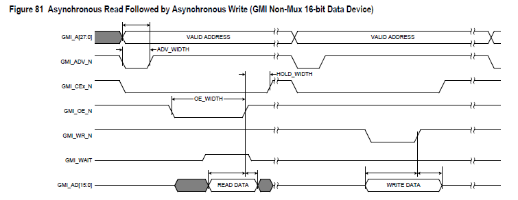
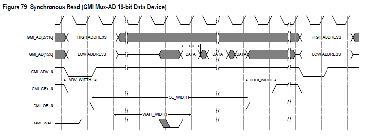
Thank you.

Below is the code. I hope, I am going in the right direction.

Is it the right way to read/Wite the Muxed INOUT bus. I have latched the
address on a rising edge and the Read/Write takes place in the falling
edge. Is it the correct way? Also, I am not sure if I have used the
Bus_Wait and Write Protect(WP) correctly.
As per the Refrence Manual:

Wait (or Ready): Level configurable input. When asserted, WAIT (RDY)
indicates the read data is invalid (Wait) or Valid (Ready). WAIT (RDY)
is driven by the devices when CEx_N and OE_N are low and High-Z when
when CEx_N or OE_N are high.

Write Protect: Active low output. When low, WP_N enables the device lock
down mechanism, or inhibits write cycles.

The timing diagrams are attached. (Following sync read in which data is
read at the falling edge )
1 | entity Mem_IF is |
2 | |
3 | Port ( |
4 | RO_Register_0 : in STD_LOGIC_VECTOR(15 downto 0); |
5 | RO_Register_1 : in STD_LOGIC_VECTOR(15 downto 0); |
6 | RO_Register_2 : in STD_LOGIC_VECTOR(15 downto 0); |
7 | |
8 | BCLK : in STD_LOGIC; |
9 | n_Reset: in STD_LOGIC; |
10 | n_OE : in STD_LOGIC; |
11 | n_WE: in STD_LOGIC; |
12 | ALE: in STD_LOGIC; |
13 | Bus_Wait: out STD_LOGIC; |
14 | n_WP: in STD_LOGIC; |
15 | n_CS_0: in STD_LOGIC; |
16 | |
17 | WR_Register_0 : out STD_LOGIC_VECTOR(15 downto 0); |
18 | WR_Register_1 : out STD_LOGIC_VECTOR(15 downto 0); |
19 | WR_Register_2 : out STD_LOGIC_VECTOR(15 downto 0); |
20 | |
21 | Add_Data: inout STD_LOGIC_VECTOR(15 downto 0) |
22 | |
23 | );
|
24 | |
25 | end Mem_IF; |
26 | |
27 | architecture Behavioral of Mem_IF is |
28 | |
29 | signal latched_addr : std_logic_vector (15 downto 0); |
30 | signal data_out : std_logic_vector (15 downto 0); |
31 | |
32 | begin
|
33 | |
34 | Add_Data <= data_out when (n_CS_0 = '0' and n_OE = '0' and n_WE = '1') else (others=>'Z'); |
35 | |
36 | latch_addr : process (BCLK, n_Reset) is |
37 | begin
|
38 | if(n_reset = '0') then |
39 | latched_addr <= (others=>'0'); |
40 | |
41 | elsif (rising_edge(BCLK)) then |
42 | if (n_CS_0 = '0' and ALE = '1') then |
43 | |
44 | latched_addr <= Add_Data; |
45 | end if; |
46 | end if; |
47 | end process latch_addr; |
48 | |
49 | |
50 | MEM_READ : process (BCLK, n_Reset) is |
51 | begin
|
52 | if(n_reset = '0') then |
53 | Bus_Wait <= '0'; |
54 | data_out <= (others=>'0'); |
55 | |
56 | elsif (falling_edge(BCLK)) then |
57 | if (n_CS_0 = '0' and n_WE = '1' and n_OE = '0' and ALE = '0') then |
58 | CASE (latched_addr) IS |
59 | |
60 | WHEN H"00" => data_out <= RO_Register_0; |
61 | WHEN H"01" => data_out <= RO_Register_1; |
62 | WHEN H"02" => data_out <= RO_Register_2; |
63 | |
64 | WHEN OTHERS => data_out <= (others=>'0'); |
65 | |
66 | |
67 | END CASE; |
68 | |
69 | Bus_Wait <= '1'; |
70 | end if; |
71 | end if; |
72 | end process MEM_READ; |
73 | |
74 | |
75 | MEM_WRITE : process (BCLK, n_Reset) is |
76 | begin
|
77 | if(n_Reset = '0') then |
78 | Bus_Wait <= '0'; |
79 | data_out <= (others=>'0'); |
80 | |
81 | elsif (falling_edge(BCLK)) then |
82 | if (n_CS_0 = '0' and n_WE = '0' and n_OE = '1' and n_WP = '1' and ALE = '0') then |
83 | |
84 | Bus_Wait <= '0'; |
85 | |
86 | CASE (latched_addr) IS |
87 | |
88 | WHEN H"10" => WR_Register_0 <= Add_Data; |
89 | WHEN H"10" => WR_Register_1 <= Add_Data; |
90 | WHEN H"10" => WR_Register_2 <= Add_Data; |
91 | |
92 | WHEN OTHERS => data_out <= (others=>'0'); |
93 | |
94 | |
95 | END CASE; |
96 | end if; |
97 | end if; |
98 | end process MEM_WRITE; |
99 | |
100 | end Behavioral; |
I would assume your manual should have a bus state diagram and I would
also assume you'll probably need a state machine on the FPGA side that
would resemble it.

Other than that, you'll most likely need a testbench to verify you have
implemented the state machine correctly.

Without the detailed specs (no, I'm not going to read or even download
it) it is difficult to be more specific.
Please log in before posting. Registration is free and takes only a minute.
Existing account
Do you have a Google/GoogleMail account? No registration required!
Log in with Google account
Log in with Google account
No account? Register here.