Hello ALL,

I am a beginner with fpga boards.I have a code and i need to run it on
BASYS 2 board . Basically its a code for generating gating signals. I
need help how to assign input and output ports and how do i check
whether i am getting correct output.
Attached is the code for reference.

Help will e highly appreciated.
Nirav B. wrote:
> I need help how to assign input and output ports
What toolchain?

> and how do i check whether i am getting correct output.
Wrap a testbench around your module and apply some stimuli signals.

One thing you will find out is that you will get some spurios gating
signals when changing the half_duty randomly. This is because you
compare the switching points by equalitiy:
1 | IF(count(i) = half_duty) THEN |
2 | G1_out(i) <= '0'; |
3 | ELSIF(count(i) = half_duty +10 ) then |
4 | G2_out(i) <= '1'; |
5 | ELSIF (count(i) = period - half_duty -10) THEN |
6 | G2_out(i) <= '0'; |
7 | ELSIF(count(i) = period - half_duty) THEN |
8 | G1_out(i) <= '1'; |
9 | END IF; |
Better would be to change half_duty only when the counter is reset to 0.
Or at least you must change the half_duty value at a point where all
phases are in an inactive state...

BTW: pls attach a VHDL file as *.vhd or *.vhdl (not as *.txt)
You will see some little magic named "syntax highlighting"...
Attached files:
-

20160415_151736.jpg
240 KB -

Capture.JPG
72 KB
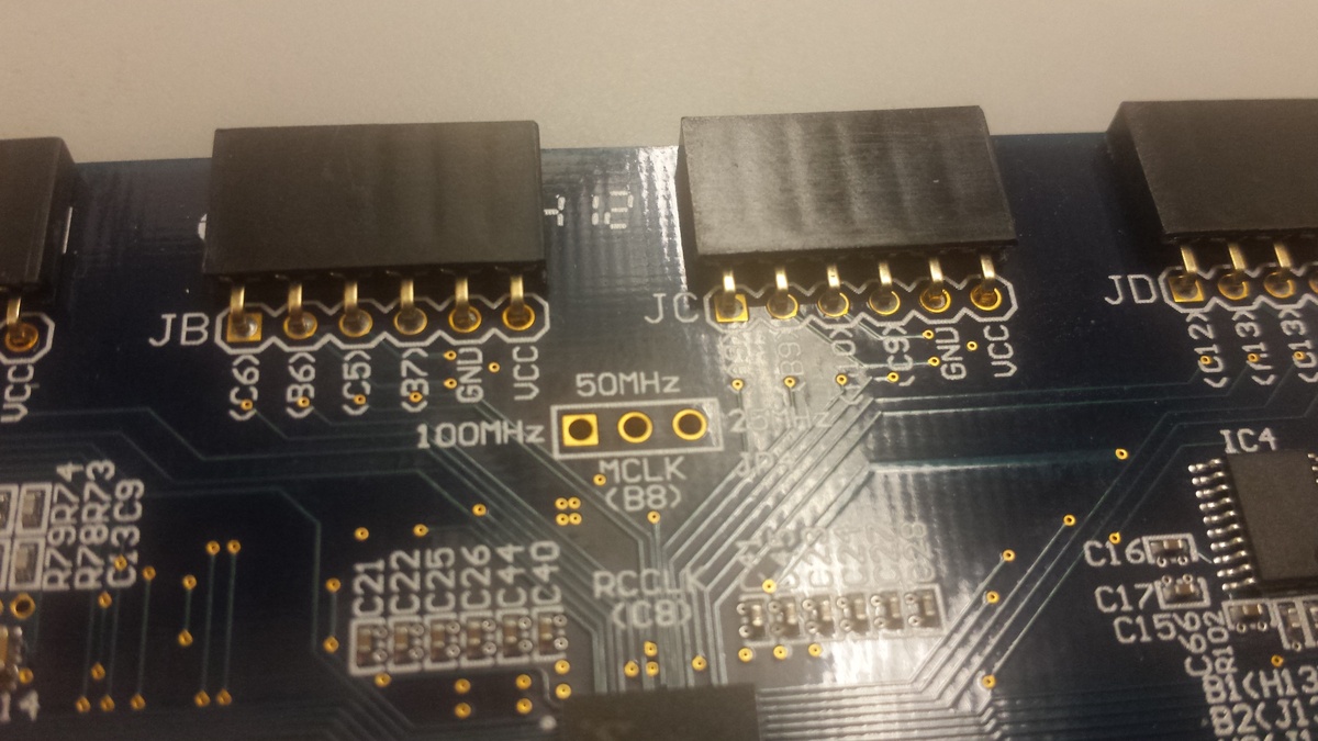
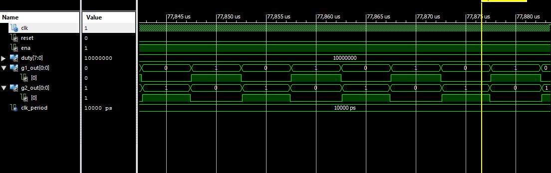
I am sorry for late reply.Exams compelled me to stay away from this
board.

I am not sure what tool chain means..... I guess i assigned them in plan
ahead also i did not get what you mean by wrapping up test bench.

Attached are the.vhd file and .ucf file for input and output port pins.

1. I am not sure of clock signal.The clock i have used is 50 MHz and the
pin B8 on board says it gives 50 MHz , i am really not sure how to check
the clock.Attached is the image of the board where clock is shown.

2. I should get results like atttached ISIM snapshot. G1 and G2 output
should be conducting at 50% duty cycle.

I am dumbest ever guy in FPGA but i want to learn and get better at it.

Please help me.
Please log in before posting. Registration is free and takes only a minute.
Existing account
Do you have a Google/GoogleMail account? No registration required!
Log in with Google account
Log in with Google account
No account? Register here.