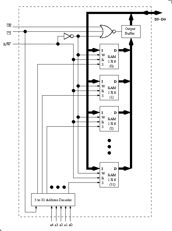
Hey guys I am trying to implement a 32x6RAM in VHDL and I swear
everything looks fine when after going through my source code but I
can't seem to figure out why I get a dangling signal/multiple source
error when I try to create S=>AD(0) to S=>AD(31)...Can anyone help me
point out what I may be forgetting in my code please?

Code:
library IEEE;
use IEEE.STD_LOGIC_1164.ALL;
use IEEE.STD_LOGIC_ARITH.ALL;
use IEEE.STD_LOGIC_UNSIGNED.ALL;

--Uncomment the following library declaration if instantiating
--any Xilinx primitives in this code.
--library UNISIM;
--use UNISIM.VComponents.all;

entity mm32by6RAM is
    Port ( OE   : in    STD_LOGIC;
           CS   : in    STD_LOGIC;
           RW   : in    STD_LOGIC;
           A    : in    STD_LOGIC_VECTOR (4 downto 0);
           D    : out   STD_LOGIC_VECTOR (5 downto 0));
end mm32by6RAM;

architecture Behavioral of mm32by6RAM is

COMPONENT mm5to32Decoder
    Port ( A    : in    STD_LOGIC_VECTOR (4 downto 0);
           OEB : in     STD_LOGIC;
           Z    : out   STD_LOGIC_VECTOR (31 downto 0));
end COMPONENT;


COMPONENT mm1by6RAM
    Port ( I : in   STD_LOGIC_VECTOR (5 downto 0);
           W : in   STD_LOGIC;
           R : in   STD_LOGIC;
           S : in   STD_LOGIC;
              D : out   STD_LOGIC_VECTOR (5 downto 0));
end COMPONENT;


COMPONENT mmOutputBuffer
    Port ( B    : in    STD_LOGIC_VECTOR(5 downto 0);
           OE   : in    STD_LOGIC;
           D    : out   STD_LOGIC_VECTOR (5 downto 0));
end COMPONENT;


COMPONENT mm3NOR
    Port ( A : in   STD_LOGIC;
           B : in   STD_LOGIC;
           C : in   STD_LOGIC;
           Z : out      STD_LOGIC);
end COMPONENT;


COMPONENT mmINVERT
    Port ( a : in       STD_LOGIC;
           z : out      STD_LOGIC);
end COMPONENT;


SIGNAL RWnot        :   STD_LOGIC;
SIGNAL N                :   STD_LOGIC;
SIGNAL OB           :   STD_LOGIC_VECTOR (5 downto 0);
SIGNAL AD           :   STD_LOGIC_VECTOR (31 downto 0);
SIGNAL Ram          :   STD_LOGIC_VECTOR (5 downto 0);

begin

gate1       :   mmINVERT            PORT MAP    (a=>RW,     z=>RWnot);
gate2       :   mm3NOR          PORT MAP    (A=>OE,     B=>CS,
C=>RWnot,   Z=>N);
gate3       :   mmOutputBuffer  PORT MAP    (B=>Ram, OE=>N,
D=>OB);
gate4       :   mm5to32Decoder  PORT MAP    (A=>A,  OEB=>CS,
Z=>AD);

gate5       :   mm1by6RAM       PORT MAP    (I=>OB,     W=>RWnot,
R=>RW,  S=>AD(0),   D=>Ram);
gate6       :   mm1by6RAM       PORT MAP    (I=>OB, W=>RWnot,   R=>RW,
S=>AD(1),   D=>Ram);
--gate7     :   mm1by6RAM       PORT MAP    (I=>OB, W=>RWnot,   R=>RW,
S=>AD(2),   D=>Ram);
--gate8     :   mm1by6RAM       PORT MAP    (I=>OB, W=>RWnot,   R=>RW,
S=>AD(3),   D=>Ram);
--gate9     :   mm1by6RAM       PORT MAP    (I=>OB, W=>RWnot,   R=>RW,
S=>AD(4),   D=>Ram);
--gate10    :   mm1by6RAM       PORT MAP    (I=>OB, W=>RWnot,   R=>RW,
S=>AD(5),   D=>Ram);
--gate11    :   mm1by6RAM       PORT MAP    (I=>OB, W=>RWnot,   R=>RW,
S=>AD(6),   D=>Ram);
--gate12    :   mm1by6RAM       PORT MAP    (I=>OB, W=>RWnot,   R=>RW,
S=>AD(7),   D=>Ram);
--gate13    :   mm1by6RAM       PORT MAP    (I=>OB, W=>RWnot,   R=>RW,
S=>AD(8),   D=>Ram);
--gate14    :   mm1by6RAM       PORT MAP    (I=>OB, W=>RWnot,   R=>RW,
S=>AD(9),   D=>Ram);
--gate15    :   mm1by6RAM       PORT MAP    (I=>OB, W=>RWnot,   R=>RW,
S=>AD(10),  D=>Ram);
--gate16    :   mm1by6RAM       PORT MAP    (I=>OB, W=>RWnot,   R=>RW,
S=>AD(11),  D=>Ram);
--gate17    :   mm1by6RAM       PORT MAP    (I=>OB, W=>RWnot,   R=>RW,
S=>AD(12),  D=>Ram);
--gate18    :   mm1by6RAM       PORT MAP    (I=>OB, W=>RWnot,   R=>RW,
S=>AD(13),  D=>Ram);
--gate19    :   mm1by6RAM       PORT MAP    (I=>OB, W=>RWnot,   R=>RW,
S=>AD(14),  D=>Ram);
--gate20    :   mm1by6RAM       PORT MAP    (I=>OB, W=>RWnot,   R=>RW,
S=>AD(15),  D=>Ram);
--gate21    :   mm1by6RAM       PORT MAP    (I=>OB, W=>RWnot,   R=>RW,
S=>AD(16),  D=>Ram);
--gate22    :   mm1by6RAM       PORT MAP    (I=>OB, W=>RWnot,   R=>RW,
S=>AD(17),  D=>Ram);
--gate23    :   mm1by6RAM       PORT MAP    (I=>OB, W=>RWnot,   R=>RW,
S=>AD(18),  D=>Ram);
--gate24    :   mm1by6RAM       PORT MAP    (I=>OB, W=>RWnot,   R=>RW,
S=>AD(19),  D=>Ram);
--gate25    :   mm1by6RAM       PORT MAP    (I=>OB, W=>RWnot,   R=>RW,
S=>AD(20),  D=>Ram);
--gate26    :   mm1by6RAM       PORT MAP    (I=>OB, W=>RWnot,   R=>RW,
S=>AD(21),  D=>Ram);
--gate27    :   mm1by6RAM       PORT MAP    (I=>OB, W=>RWnot,   R=>RW,
S=>AD(22),  D=>Ram);
--gate28    :   mm1by6RAM       PORT MAP    (I=>OB, W=>RWnot,   R=>RW,
S=>AD(23),  D=>Ram);
--gate29    :   mm1by6RAM       PORT MAP    (I=>OB, W=>RWnot,   R=>RW,
S=>AD(24),  D=>Ram);
--gate30    :   mm1by6RAM       PORT MAP    (I=>OB, W=>RWnot,   R=>RW,
S=>AD(25),  D=>Ram);
--gate31    :   mm1by6RAM       PORT MAP    (I=>OB, W=>RWnot,   R=>RW,
S=>AD(26),  D=>Ram);
--gate32    :   mm1by6RAM       PORT MAP    (I=>OB, W=>RWnot,   R=>RW,
S=>AD(27),  D=>Ram);
--gate33    :   mm1by6RAM       PORT MAP    (I=>OB, W=>RWnot,   R=>RW,
S=>AD(28),  D=>Ram);
--gate34    :   mm1by6RAM       PORT MAP    (I=>OB, W=>RWnot,   R=>RW,
S=>AD(29),  D=>Ram);
--gate35    :   mm1by6RAM       PORT MAP    (I=>OB, W=>RWnot,   R=>RW,
S=>AD(30),  D=>Ram);
--gate36    :   mm1by6RAM       PORT MAP    (I=>OB, W=>RWnot,   R=>RW,
S=>AD(31),  D=>Ram);


end Behavioral;


thanks guys!
I get errors, because the entities mmInvert ....
are not defined.

Error: Node instance "gate1" instantiates undefined entity "mmINVERT"


Is this your complete source?
mike mr wrote:> everything looks fine when after going through my source code but I> can't seem to figure out why I get a dangling signal/multiple source> error when I try to create S=>AD(0) to S=>AD(31)...Can anyone help me> point out what I may be forgetting in my code please?
Look for Z=>AD
and for S=>AD(0) ... S=>AD(31)
Thats a classical multi source with two drivers on one signal.
> Hey guys I am trying to implement a 32x6RAM in VHDL
Why doing it the hard and stony way with thousands of manually
instantiated and handwired parts? Why not just using a RAM in
traditional style?
1
libraryIEEE;
2
useIEEE.STD_LOGIC_1164.ALL;
3
useIEEE.numeric_std.all;-- get rid of that old STD_LOGIC_ARITH libs!
BTW: the OE Signal is not necessary for this kind of async RAM. Its just
a kind of additional CS signal here. Tell that your teacher.
Let him/her answer this question: what has the CS signal to do inside
the Adress decoder? Why not adding the OE to the adress decoder also?
Haha I appreciate your insight. The class is a senior level logic design
course which honestly isn't all that hard. However, the projects is
where the class becomes extremely time consuming as you can see...doing
a behavioral set-up like you just showed is a much easier way to
approach this, but we are strictly doing structural VHDL. I'm assuming
this is because he wants students to understand how all the parts play
together and such. The current format is how it must be done and the
project is due tomorrow at midnight. I feel if I can just fix this
multi-source issue I will be in the clear to create the final component
(64x6RAM).

I don't see how this multi-sourcing issue works. I figure the 5to32
decoder will disable 31 1x6RAMs while enabling one 1x6RAM. So having the
AD signal the way I wrote it makes sense but I am obviously a novice at
this.

If you understand my thinking on how this code works would you be able
to tell me what I should do to avoid/fix this multi-sourcing issue? I
have done c++/C/C#, and java but VHDL is not my cup of tea even though
it is not hard. I am new to VHDL and I can't see how to get around this
problem. The professor is helpful but wont give me the info that I need
to solve this problem.

Thanks in advance!
Attached are the VHDL files and here is the link for the entire project
folder:

https://www.dropbox.com/s/gnjg67i5za7gopf/pj4.zip

I have run test benches on each component so im sure the components
should be fine.
>  but we are strictly doing structural VHDL.
Yes, indeed. Very impressive and almost senseless... :-o

Why don't you instantiate a AND Gate and wire it manually there:
1
Z<=not(AorBorC);
2
3
Z<=AandBandCandDandEandFafter222ps;
Are you allowed to use a behavioral statement like and or nor inside
a structural description? I cannot believe that its the intention of a
lecture to code a certain component in the most ugly way...

BTW: at least one error is found:
I am not allowed to use any behavioral statements as they are to only be
used in the basic gates like AND, OR, NOR, etc.

Thanks for spotting the error in my 1x6RAM. I must have been rushing and
over looked that.

When I create a vhdl module the IEEE libraries are automatically
inserted so I just leave them there.

My professor makes us use delays from a gate delay table he has given
us.

Would would I need to do to fix this multi source issue with only
altering the gates and signals? I cannot add any other components
unfortunately. Would I use inout for D in the 32x6RAM?

Could you show me what you would do please?
> Would I use inout for D in the 32x6RAM?
D : out STD_LOGIC_VECTOR (5 downto 0));
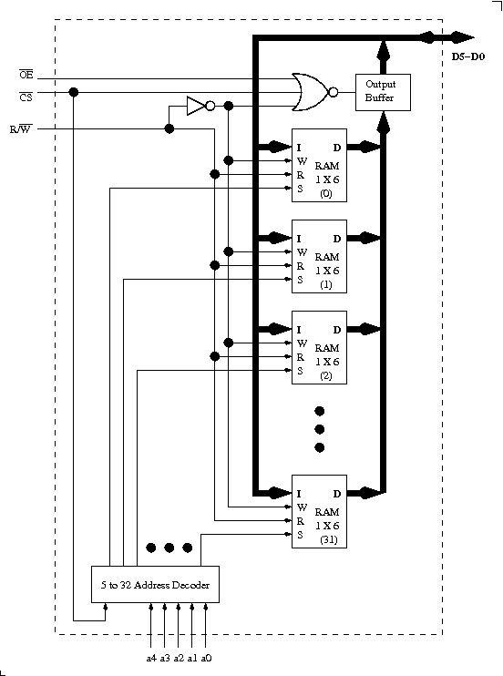
D must be inout, because the picture shows data going in and also out.
> Could you show me what you would do please?
I'm sorry, I already did...
I don't want to drill deep into a dozen of files instead of using less
than 20 lines to get the very same result.
> When I create a vhdl module the IEEE libraries are automatically> inserted
You can change that behavior:
http://www.lothar-miller.de/s9y/archives/27-Xilinx-New-Source.html
It in German, try the google translator... ;-)
Ok so I finally got everything to work HOWEVER I was wondering if you
could help me out debug these warnings. I have to do multiple test
benches on this program so I want to make sure everything is working
properly.
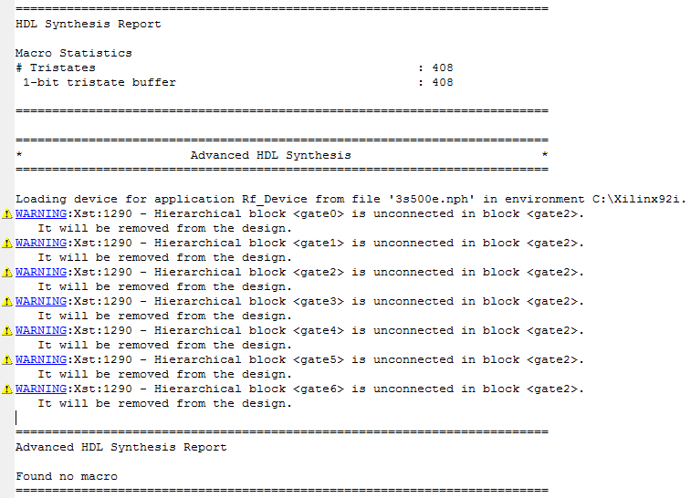
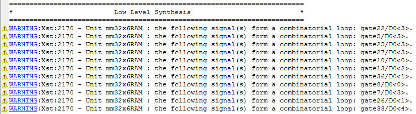
Ok so I get combinatorial loops in the mm32x6RAM module (gates 5-36),
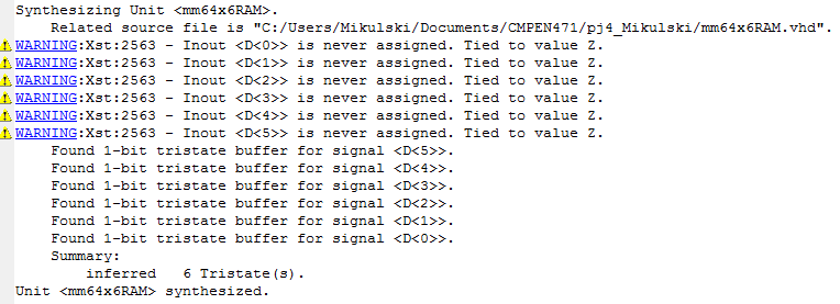
Inout D(0)-D(5) is never assigned. tied to value Z in the 64x6RAM
module, and some weird error I have never seen before.
I have attached images of the errors and the vhdl files that correspond
to the errors
There you have three very elementary problems:
First unused signals. That may be a result of a problem elsewhere,
having as a consequence that the now mentioned signals are unused.

Then a combinational loop. That may be a result of switching the
direction is not working properly.

And last the unassigned D. Thats the most astonishing thing. Something
with the disabling of the ports ist not working properly. That may cause
the first problem.

So, now what oyu MUST do is a simulation of your design! It makes
absolutely no sense to try to synthesize such a scattered design and try
to track down each one of the hundreds of signals inside...

I changed my design to 64 words RAM:
1
libraryIEEE;
2
useIEEE.STD_LOGIC_1164.ALL;
3
useIEEE.numeric_std.all;-- get rid of that old STD_LOGIC_ARITH libs!
And: my design works as expected.

You can adapt this testbench to your needs simply by changing some
names. And then you can check whats different between your design and
mine, and why yours is not working...
